Solid-state imaging device and method for manufacturing the same

a technology of solid-state imaging and manufacturing methods, which is applied in the direction of color television, television systems, radio control devices, etc., can solve the problems of spacer and solid-state imaging devices distorted, damage to solid-state imaging devices, and inability to work properly

Inactive Publication Date: 2004-09-30
FUJIFILM CORP +1
View PDF26 Cites 16 Cited by
  • Summary
  • Abstract
  • Description
  • Claims
  • Application Information

AI Technical Summary

Problems solved by technology

Moreover, since the spacer is pressed onto the solid-state imaging device to generate a stress during the bonding process, the spacer and the solid-state imaging device are distorted.
Furthermore, because the solid-state imaging element generates much heat when the solid-state imaging device is operated at a high clock rate or takes an image for a long exposure time, the difference in thermal expansion rate between the solid-state imaging element chip and the spacer causes stress.
In bonding the spacer to the wafer, if the adhesives are flowed on the solid-state imaging element chip, the solid-state imaging device does not work properly because of noise interference caused by the flowed adhesive.
Moreover, if the gap between the spacer and the wafer is not tightly sealed, the solid-state imaging device is damaged by cooling water during the dicing process.
Although a small amount of adhesive with high viscosity is dropped on the spacer by potting method according to the above publication, putting the adhesives on the spacer having the width less than 200 .mu.m is technically difficult.
Even if the spacer has the width more than 200 .mu.m, dropping the adhesives on all bonded surface

Method used


Image

  • Solid-state imaging device and method for manufacturing the same
  • Solid-state imaging device and method for manufacturing the same
  • Solid-state imaging device and method for manufacturing the same

Examples


Embodiment Construction

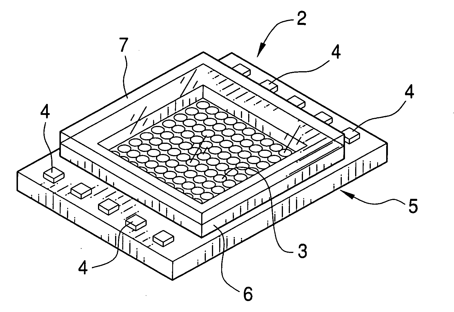
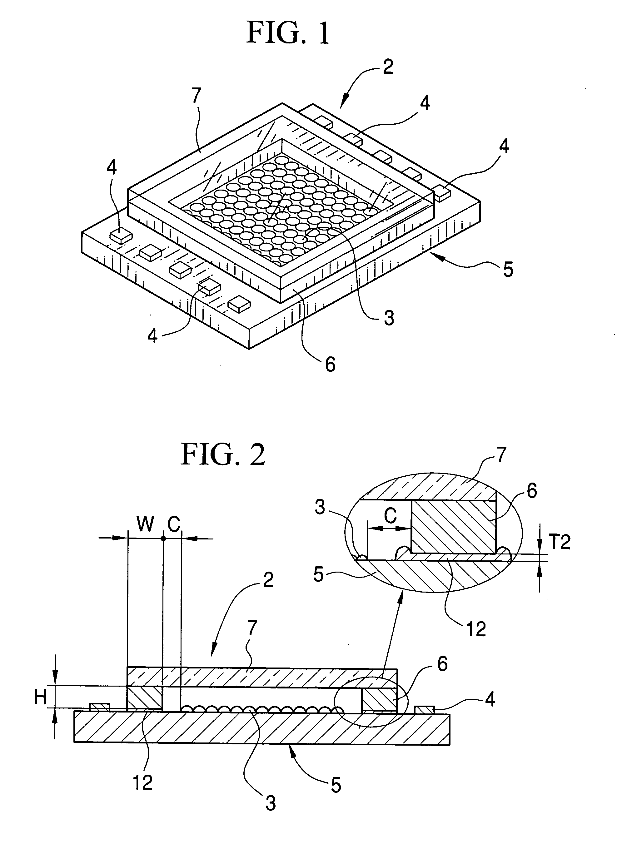
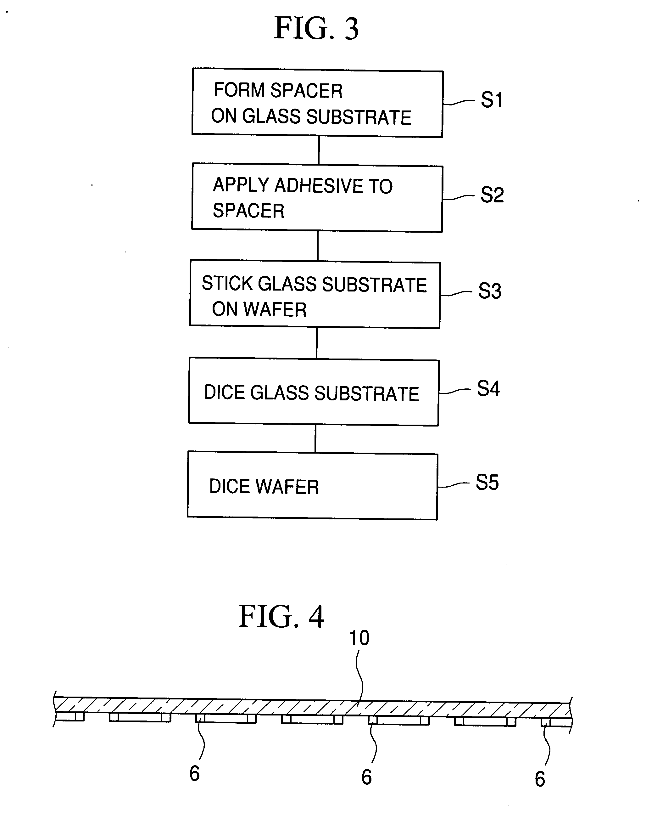
[0049] FIGS. 1 and 2 respectively show the perspective and partial cross section of a solid-state imaging device of the wafer level CPS structure that is manufactured by the method according to the present invention. The solid-state imaging device 2 comprises a solid-state imaging element 3, a rectangular-shaped solid-state imaging element chip 5, a frame-shaped spacer 6 and a cover glass 7. The solid-state imaging element 3 is coupled to the solid-state imaging element chip 5 via plural terminals 4 formed on the solid-state imaging element chip 5. The spacer 6, bonded to the solid-state imaging element chip 5, surrounds the solid-state imaging element 3. The cover glass 7 is provided on the spacer 6 to seal the solid-state imaging element 3. The cover glass 7 is made from a transparent .alpha.-ray shielding glass for the purpose of protecting the photo-diodes of the CCD.

[0050] An example of the solid-state imaging element 3 is a charge coupled device (CCD). There are color filters ...


PUM


Abstract

A transfer film, on which an adhesive is applied, is glued to plural spacers formed on a glass substrate. The glass substrate is laid on a working table, and one end of the transfer film is fixed to a winding roller. A peeling guide is set at a position over the transfer film. The winding roller is driven to wind the transfer film while the working table moves horizontally. While winding the transfer film, the angle between the glass substrate and the transfer film is kept constant. After the transfer film is peeled off, the adhesive is uniformly transferred to each of the spacers.

Description

[0001] 1. Field of the Invention[0002] The present invention relates to a method for manufacturing a solid-state imaging device by use of wafer level chip size packaging technique, and a solid-state imaging device manufactured by such manufacturing method.[0003] 2. Description of the Related Art[0004] Digital cameras, equipped with a solid-state imaging device and a semiconductor memory device, are widely spread among consumers. In addition, small electric apparatus, such as a mobile phone and a personal digital assistance (PDA), has the solid-state imaging device and the memory device to enable digital photography. A conventional solid-state imaging device is manufactured by the following steps. First, a solid-state imaging element chip, such as a charge coupled device (CCD) formed on a wafer, is die-bonded on a package formed from a ceramic, for instance. Then, after the terminals of the solid-state imaging element chip and the terminals of the package are electrically connected b...

Claims


Application Information

Patent Timeline
IPC IPC(8): H01L27/14H01L27/146H01L31/0203H04N5/335
CPCH01L27/146H01L27/14683H01L27/14618H01L2924/0002H01L2924/16235H01L2924/00
Inventor TAKASAKI, KOSUKENISHIDA, KAZUHIROYAMAMOTO, KIYOFUMI
Owner FUJIFILM CORP
Why Eureka
Try Eureka