Solid-state imaging device, driving method thereof, and camera

Inactive Publication Date: 2009-06-25
PANASONIC CORP
View PDF8 Cites 14 Cited by
  • Summary
  • Abstract
  • Description
  • Claims
  • Application Information

AI Technical Summary

Benefits of technology

[0036]As the above description has clarified, the solid-state imaging device in the present invention and a driving method thereof allows a well region in the vicinity of a read-out gate to be formed with dopant concentration thereof lowered, which facilitates a read-out operation of signal charge. Further, an effect of the MIDDLE level voltage of the column transfer clocks shifted to minus allows a potential barrier at a gate part to be enlarged in a state

Problems solved by technology

A typical disadvantage caused by the conventional solid-state imaging device and the method thereof is that potential control at a gate portion (well region near the read-out gate) becomes difficult due to reduction of the area of a region in which the read-out gate is formed.
In other words, even though enough distance and dopant concentration are essential in order to form an isolation between a photodiode and a column CCD, the miniaturization fails to keep the distance, and an enough potential barrier cannot be secured between the photodiode and the column CCD.

Method used


Image

  • Solid-state imaging device, driving method thereof, and camera
  • Solid-state imaging device, driving method thereof, and camera
  • Solid-state imaging device, driving method thereof, and camera

Examples


first embodiment

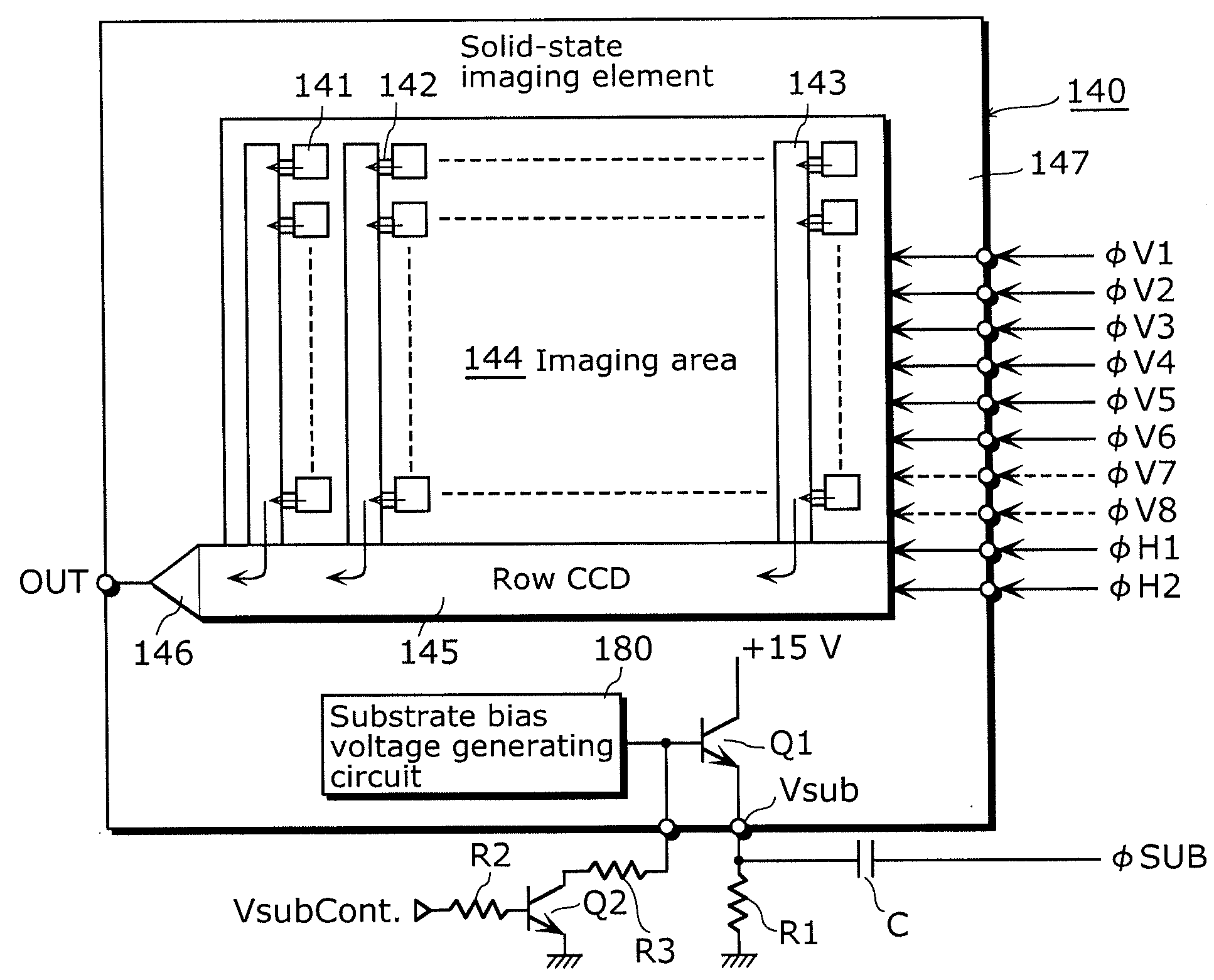
[0096]FIG. 5 shows a structure of a camera (imaging device) using a solid-state imaging device in a first embodiment.

[0097]As shown in FIG. 5, a camera 101 includes: a lens 110 forming an optical image of an object on a solid-state imaging element; an optical system 120, such as a mechanical shutter and a mirror optically processing the optical images passing through the lens 110; a solid-state imaging device 130 in the present invention; a signal processing unit 160; and a digital signal processor (referred also to as “DSP”, hereinafter) 170.

[0098]The solid-state imaging device 130 includes a solid-state imaging element 140 and a driving pulse controlling unit 150.

[0099]The solid-state imaging element 140, such as an CCD image sensor, generates a pixel signal in accordance with an amount of received light.

[0100]Following a direction from the DSP 170, the driving pulse controlling unit 150 controls the solid-state imaging element 140 by generating various driving pulses at various s...

second embodiment

[0137]FIG. 12 shows a structure of a camera (imaging apparatus) 201 in a second embodiment.

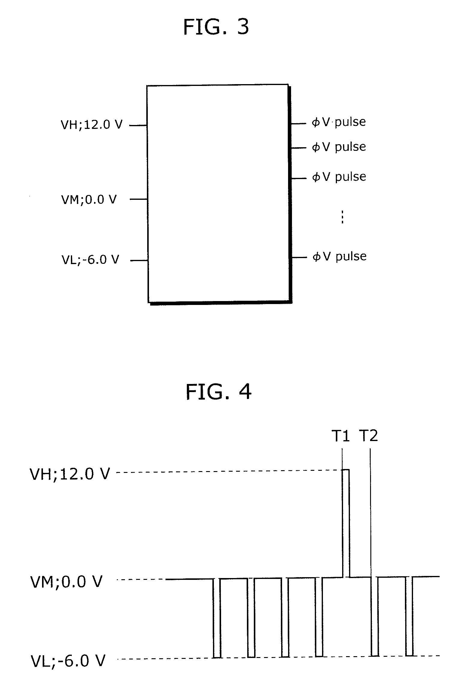
[0138]The camera 201 in the embodiment is different from the camera 101 in the first embodiment in that the camera 201 includes a driving pulse controlling unit 250 which has a different structure from the driving pulse controlling unit 150 in the first embodiment. The driving pulse controlling unit 250 includes a driving pulse generating unit 252 and a pulse shifting unit 253. The pulse shifting unit 253 has a circuit part which is shared with the solid-state imaging element 140.

[0139]FIGS. 13A and 13B illustrate a structure of the driving pulse controlling unit 250. It is noted that FIG. 13B only shows a structure to generate a column transfer clock φV1 in FIG. 13A. This structure is similar to a structure to generate column transfer clocks φV2 to φV6.

[0140]The driving pulse controlling unit 250 has no −1 V power supply, and thus has a similar structure to a power source of the driving pulse...

third embodiment

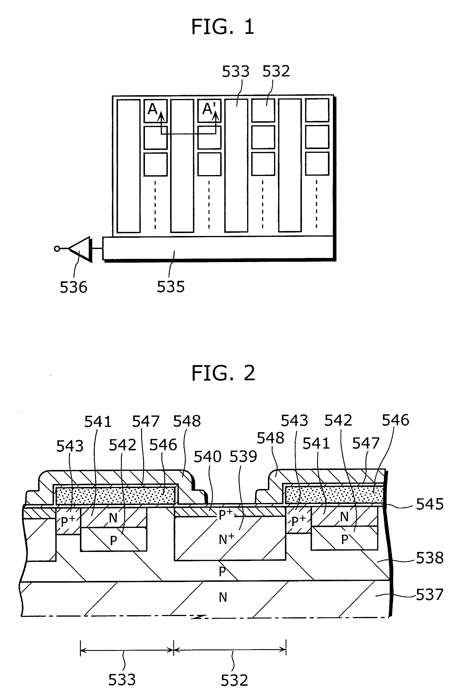
[0155]FIG. 17 is a cross-sectional view of a solid-state imaging element 340 in a third embodiment. In particular, FIG. 17 is a cross-sectional view showing a structure of the photodiode 341 and the column CCD 143 in a substrate in-depth direction.

[0156]The solid-state imaging element 340 in the embodiment is different from the solid-state imaging element 140 in the first embodiment in that the solid-state imaging element 340 includes a photodiode 341 having a different cross-sectional structure from that of the photodiode 141 in the first embodiment. The photodiodes 341 is structured to have the signal charge accumulating region 192 and a hole storage region 393. The signal charge accumulating region 192 and the hole storage region 393 are located beside the charge transfer region 195. A side portion, of the hole storage region 393, facing to the charge transfer region 195 recedes in a direction away from the charge transfer region 195 with respect to a side portion, of the signal ...


PUM


Abstract

An objective of the present invention is to provide the solid-state imaging device and the driving method thereof which can control: a poor picture quality, such as blooming, to maximize a dynamic range of the photodiode; and a poor picture quality resulted from an incomplete read-out operation. A solid-state imaging device in the present invention includes: a solid-state imaging element; and a driving pulse controlling unit applying a driving pulse to each of read-out gates of a column CCD. The driving pulse controlling unit transfers in a column direction signal charge within a charge transfer region of the column CCD by applying a column transfer clock having a LOW level voltage and a MIDDLE level voltage, and the LOW level voltage and the MIDDLE level voltage are minus voltages.

Description

BACKGROUND OF THE INVENTION[0001](1) Field of the Invention[0002]The present invention relates to solid-state imaging devices, such as a CCD image sensor, and driving methods thereof, and particularly to a technique for isolating a photodiode.[0003](2) Description of the Prior Art[0004]Recent solid-state imaging devices have achieved high-pixel density of 10 million pixels or more, which allows the users to record a still picture as clear as a picture taken on silver film, and a moving picture. Along with the introduction of the devices having the high-pixel density, a pitch of a unit pixel size of a solid-state imaging device becomes smaller than 2 μm, and the unit pixel size continues to be miniaturized. With reference to an interline-transfer solid-state imaging device (ITCCD) as an example, a structure of a conventional solid-state imaging device and a driving method thereof (Patent Reference: Japan Unexamined Patent Application Publication No. 2005-93915) shall be described her...

Claims


Application Information

Patent Timeline
IPC IPC(8): H04N5/335H01L27/148H04N5/355H04N5/359H04N5/361H04N5/367H04N5/372
CPCH04N5/335H04N5/3765H04N5/372H04N25/00H04N25/71H04N25/745
Inventor KATO, YOSHIAKIKOHNO, AKIYOSHIMATSUMOTO, HIROSHIFUJITA, TAKESHI
Owner PANASONIC CORP
Why Eureka
Try Eureka