Method and device for preventing damage to a semiconductor switch circuit during a failure

a technology of semiconductor switch circuit and protection device, which is applied in the direction of protective switch using micromechanics, contact, emergency protective circuit arrangement, etc., can solve the problems of short circuit, failure such as these, and damage to the igbt module or the physical equipment, so as to prevent damage

Inactive Publication Date: 2009-06-25
GENERAL ELECTRIC CO
View PDF7 Cites 20 Cited by
  • Summary
  • Abstract
  • Description
  • Claims
  • Application Information

AI Technical Summary

Benefits of technology

[0013]In accordance with an embodiment of the present invention, a device comprises at least one semiconductor switching circuit connected to a power source and load and at least one breaker switch integrated with the at least one semiconductor switching circuit. The breaker circuit may be connected in series wit...

Problems solved by technology

A problem arises with the use of the IGBT modules where the semiconductor switch looses its voltage blocking capability causing a short circuit.
Failures such as these can have significant consequences, for example, damage to the IGBT module or to the equipment located physically near the IGBT module.
This high current amplitude leads to a thermal overload of the bond wires 9.
Standard protection equi...

Method used


Image

  • Method and device for preventing damage to a semiconductor switch circuit during a failure
  • Method and device for preventing damage to a semiconductor switch circuit during a failure
  • Method and device for preventing damage to a semiconductor switch circuit during a failure

Examples


Embodiment Construction

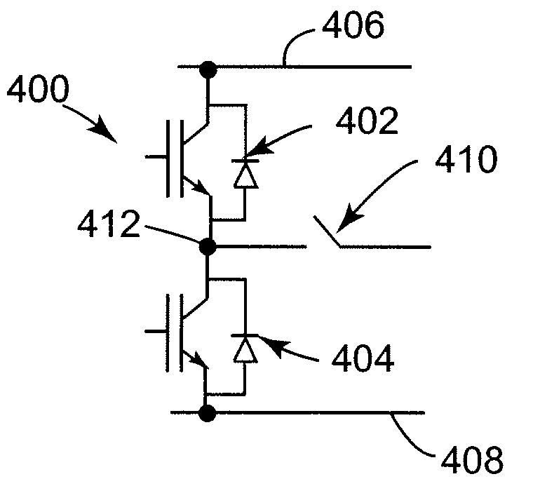
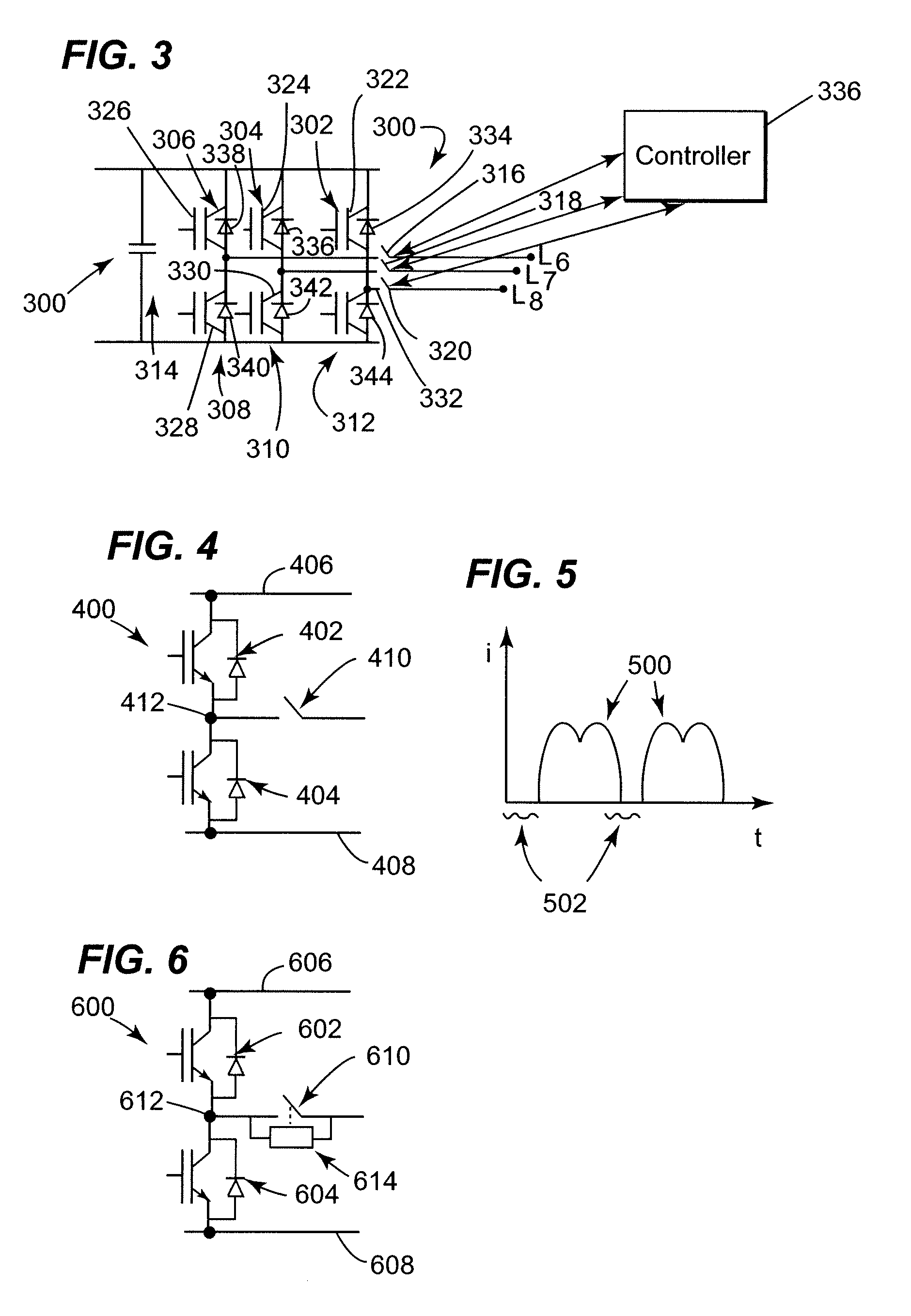
[0028]One embodiment of the present invention concerns a device and a method for preventing damage to one or more semiconductor switches by providing a breaker switch capable of creating an open circuit condition in less than about twenty microseconds of determination of an over current condition in a circuit carrying current to the semiconductor switch(es). In one particular embodiment, a microelectromechanical system (MEMS) breaker switch may be integrated into an insulated gate bipolar transistor (IGBT) module. In case a failure is detected by the main inverter control system, the MEMS breaker switch is commanded to disconnect the IGBT from all loads or power sources. Use of the MEMS breaker switch allows the current to the IGBT to be interrupted in less than about twenty microseconds (μs), especially within the IGBTs rated short circuit withstand time. By this method an explosion of the IGBT module housing is avoided. The risk for damaging neighbor devices is minimized. Bulky ex...


PUM


Abstract

A device includes at least one semiconductor switching circuit connected to a power source and a load and at least one breaker switch integrated with the at least one semiconductor switching circuit. The breaker circuit may be connected in series with the at least one semiconductor switching circuit and the at least one breaker switch is configured to create an open circuit in less than about twenty microseconds of receipt of a predetermined threshold of semiconductor switch current to thereby prevent damage to the at least one semiconductor switching circuit or housing. A method of preventing damage to a semiconductor switching circuit or device is also presented.

Description

BACKGROUND OF THE INVENTION[0001]1. Field of the Invention[0002]The present invention relates in general to power electronic circuits and, more particularly, to semiconductor switches used in power electronic circuits.[0003]2. Related Art[0004]Inverters used in variable speed drive systems and power converters typically use semiconductor switches such as insulated gate bipolar transistors (IGBT) packaged into IGBT modules.[0005]A problem arises with the use of the IGBT modules where the semiconductor switch looses its voltage blocking capability causing a short circuit. One possible reason for this type of failure is a break down of the semiconductor induced by, e.g., radiant energy. This short circuit of the semiconductor switch, leads, in turn, to a short of the connected equipment which may be a multiphase power grid, a large rotating electrical machine or internal energy storage as for example the DC link capacitor.[0006]Failures such as these can have significant consequences, ...

Claims


Application Information

Patent Timeline
IPC IPC(8): H02H3/00
CPCH01H1/0036H02H7/1227H01H2071/008H01H9/548H01L2224/48139H01L2224/4846H01L2924/13055H01L2924/00
Inventor ROESNER, ROBERTSUBRAMANIAN, KANAKASABAPATHI
Owner GENERAL ELECTRIC CO
Why Eureka
Try Eureka