Data input apparatus with improved setup/hold window

a data input apparatus and setup/hold window technology, applied in the field of semiconductor memory devices, can solve the problems of insufficient synchronous memory devices of sdr, difficult to secure data setup/hold time upon entering into test mode, and more difficult to secure data setup/hold time margins

Inactive Publication Date: 2009-06-25
SK HYNIX INC
View PDF0 Cites 16 Cited by
  • Summary
  • Abstract
  • Description
  • Claims
  • Application Information

AI Technical Summary

Benefits of technology

[0023]The present invention provides a data input apparatus in a semiconductor memory device capable of improving a setup / hold time window in a test mode.
[0024]Additionally, the present invention provides a data input apparatus capable of improving productivity by reducing the number of pins required in test equipment when testing a semiconductor memory device.
[0025]Additionally, the present invention provides a data input apparatus capable of increasing signal transmission efficiency and improving a data setup / hold time window since the output signal of the clock buffer in the present invention is not passed through a data strobe driver when the semiconductor device is in a test mode.
[0026]Additionally, the present invention controls the degree of delaying of data inputted from the external by a test mode signal.
[0044]Preferably, the degree of delay that the data delay unit delays the signal outputted from the data buffer is enough to secure setup and hold time window margins of the data when the test mode signal is enabled.

Problems solved by technology

However, the SDR synchronous memory device is insufficient when a system requires high speed operation.
However, in the prior art shown in FIG. 3, it is difficult to secure the data setup / hold time upon entering into the test mode, since the pulse signals DQSRP and DQSFP, which are used as the data alignment signal of the data alignment unit 38, are synchronized by means of the internal clock signal BCK as shown in FIG. 3.
Accordingly, it is more difficult to secure the data setup / hold time margins in the semiconductor device shown in FIG. 3.

Method used


Image

  • Data input apparatus with improved setup/hold window
  • Data input apparatus with improved setup/hold window
  • Data input apparatus with improved setup/hold window

Examples


Embodiment Construction

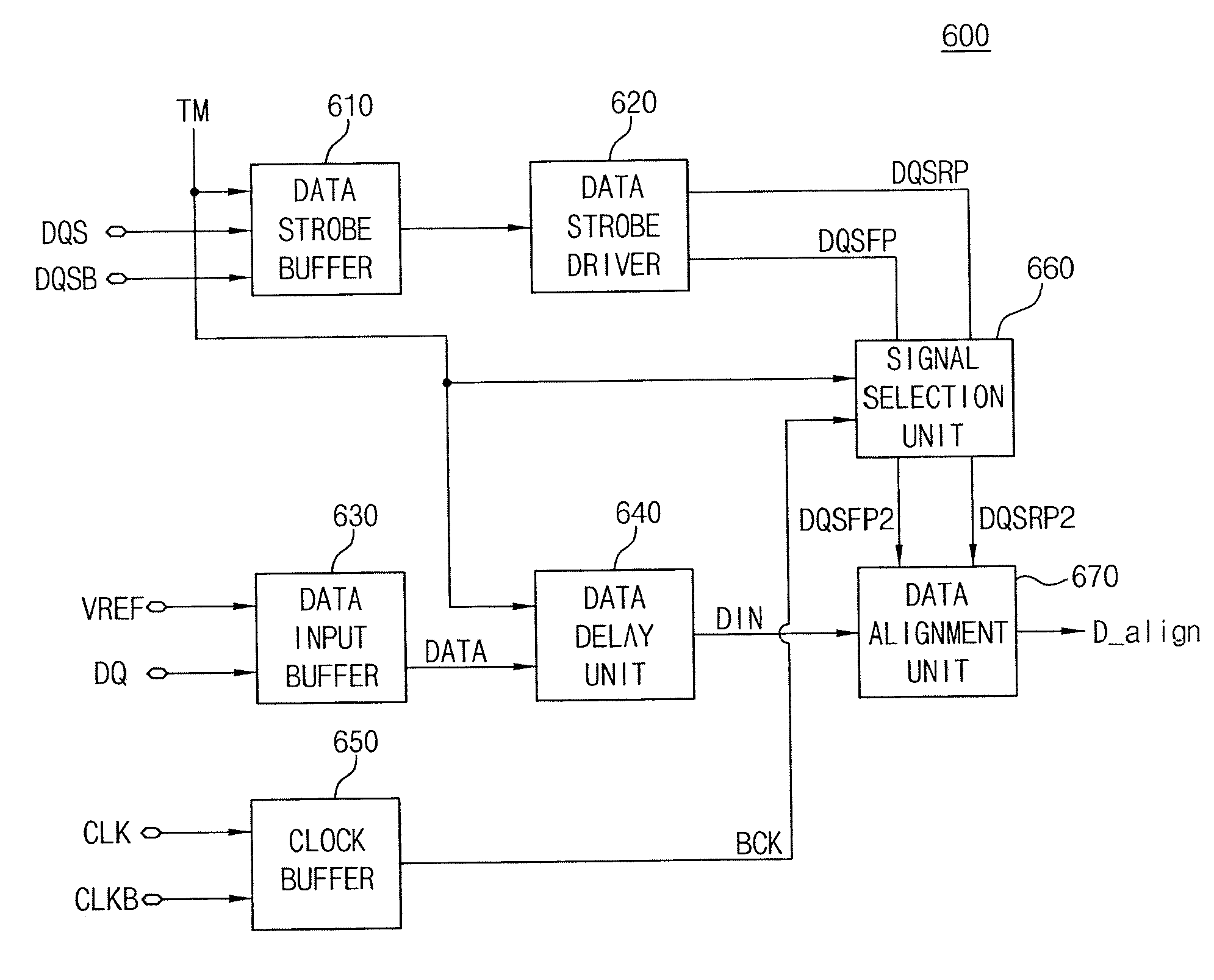
[0059]The present invention discloses: a method capable of improving a data setup / hold time window by adding a delay unit, which is capable of controlling the degree data is delayed, for improving the data setup / hold time window upon entering into a test mode; and a circuit that is synchronized with a clock buffer upon entering into the test mode and that outputs a data alignment signal to the front of a data block.

[0060]Hereinafter, preferred embodiments of the present invention will be described with reference to the accompanying drawings.

[0061]FIG. 5 is a block view schematically showing a data input apparatus according to the present invention.

[0062]Referring to FIG. 5, the data input / output apparatus 500 comprises a data delay unit 510 delaying data DQ input from the external by a predetermined time in response to a test mode signal and outputting the delayed data; a data alignment signal generating unit 520 receiving two input signals IN1 and IN2 and outputting any one of the ...


PUM


Abstract

In the data input apparatus, a data delay unit outputs data input from outside the data input apparatice. The data delay unit varies the degree of delay in response to a test mode signal. A data alignment signal generating unit receives a first signal synchronized with an external clock signal and a second signal synchronized with a data strobe signal, and the data alignment signal generating unit outputs one of the first signal and the second signal as a data alignment signal in response to the test mode signal. A data alignment unit is synchronized with the data alignment signal to align the data delayed in the data delay unit. The data input apparatus improves the setup / hold window when a semiconductor memory device is in the test mode.

Description

CROSS-REFERENCE TO RELATED APPLICATIONS[0001]The present application claims priority to Korean patent application number 10-2007-0135576 filed on Dec. 21, 2007 which is incorporated herein by reference in its entirety.BACKGROUND OF THE INVENTION[0002]The present invention relates to a semiconductor memory device, and more particularly, to a data input apparatus in a semiconductor memory device.[0003]Semiconductor memory devices are being continuously improved in order to increase the degree of integration and improve the operation speed. In order to improve operation speed, a synchronous memory device that can be operated in synchronization with a clock provided externally from a memory chip has been proposed.[0004]One such proposed synchronous memory device is a single data rate (SDR) synchronous memory device that is synchronized with a rising edge of the clock provided from the external of the memory device to input and output a single data over a single period. However, the SDR ...

Claims


Application Information

Patent Timeline
Patent Type & Authority Applications(United States)
IPC IPC(8): G11C7/00G11C8/18
CPCG11C7/1072G11C7/1078G11C7/1084G11C7/109G11C8/18G11C7/22G11C7/225G11C8/06G11C7/1093G11C11/407G11C11/4093G11C11/4096
Inventor KU, KIE BONGCHO, KWANG JUN
Owner SK HYNIX INC
Why Eureka
Try Eureka