Pulse signal delay circuit and LED drive circuit

a signal delay and led drive technology, applied in pulse manipulation, pulse technique, instruments, etc., can solve the problems of reducing the freedom of setting the frequency, unable to ignore the abnormal sounds described above, and unable to achieve the effect of preventing flickering and emission, preventing inconsistency in brightness, and preventing the effect of inconvenient operation

Inactive Publication Date: 2009-07-02
SHARP KK
View PDF8 Cites 18 Cited by
  • Summary
  • Abstract
  • Description
  • Claims
  • Application Information

AI Technical Summary

Benefits of technology

[0016]The present invention has been made in view of the problems, and a first object thereof is to provide a pulse signal delay circuit which can precisely delay the input pulse signal by a constant delay time while maintaining the duty ratio so that the LED circuit can be driven with a precise time difference. In addition, a second object of the present invention is to provide an LED drive circuit which can drive an LED circuit while preventing inconsistency in the brightness, flickering and emission of sound from a condenser without restricting the freedom in setting the frequency of the PWM signal for driving LED.
[0018]In the pulse signal delay circuit according to the first characteristics, the first edge detection delay timing generated by the first pulse edge delay circuit is gained by delaying the detection timing of the rising edge of the input pulse signal by a constant delay time a predetermined number of times, and the second edge detection delay timing generated by the second pulse edge delay circuit is gained by delaying the detection timing of the falling edge of the input pulse signal by the same delay time as that of the first edge detection delay timing a predetermined number of times, and therefore, the Mth delay pulse signal which rises according to the first edge detection delay timing gained through M (M is a natural number) times of delays generated by the delay pulse signal generating circuit and falls according to the second edge detection delay timing gained through M times of delays, and the Nth delay pulse signal which rises according to the first edge detection delay timing gained through N (N is a natural number other than M) times of delays and falls according to the second edge detection delay timing gained through N times of delays have the same pulse width between the rising edge and the falling edge, and therefore, the duty ratio can be maintained equal among all the delay pulse signals. In addition, the delay time between two delay pulse signals front and rear can be made equal. As a result, a pulse signal delay circuit can be provided which can drive an LED circuit with precise time difference and can precisely delay an input pulse signal by a constant delay time while maintaining the duty ratio.
[0020]In the pulse signal delay circuit according to the second characteristics, the first pulse edge delay circuit and the second pulse edge delay circuit can be implemented using a counter circuit. Accordingly, the setting and changing of the delay time can be easily achieved through a simple operation of only changing the delay counter value.
[0023]In the pulse signal delay circuit according to the third characteristics, the timing according to which the counter value of the third counter changes becomes the first edge detection delay timing and the timing according to which the counter value of the fourth counter changes becomes the second edge detection delay timing, and therefore, the order of the generation of the first and second edge detection delay timing (that is, how many times the timing is generated before) can be identified as the counter value of the third and fourth counters, respectively, and therefore, it becomes easy to acquire the first and second edge detection delay timing gained through the same number of times of delays in the delay pulse signal generating circuit for generating a delay pulse signal by using the first and second edge detection delay timing.
[0027]In the pulse signal delay circuit according to the fifth characteristics, it becomes possible to reduce the system load of an external apparatus by providing a delay counter value generating circuit instead of the system scale of an external apparatus increasing in the case where a delay counter value is set by the external apparatus such as a microprocessor.
[0031]In the LED drive circuit according to the above described characteristics, the delay pulse signals of which the number is the same as the predetermined number of times of delays outputted from the delay pulse signal generating circuit in the pulse signal delay circuit according to any of the above described characteristics are individually inputted into the gate of the drive transistor in each of the circuit units in the LED circuit so that the LED circuit can be driven with a time difference. As a result, it becomes possible to provide an LED drive circuit which can drive an LED circuit by preventing the inconsistency in the brightness, flickering and the emission of sound from a condenser without restricting the freedom in the setting of the frequency of the PWM signal for driving LED.

Problems solved by technology

In some cases, ceramic condensers having a relatively large capacitance used as a smoothing condenser emit abnormal sounds due to vibrations caused by the piezoelectricity of the dielectric material used in the condenser as a voltage is applied.
In particular, in a case where an IC for an LED driver having the booster circuit as described above and a smoothing condenser using ceramics are combined in an apparatus which is used in close proximity to the ear, such as a cellular phone, abnormal sounds as described above cannot be ignored.
However, the following problems arise with the method for setting the frequency of the PWM signal high as disclosed in the Japanese Unexamined Patent Publication 2006-114324.
First, the range of the frequency of the PWM signal is limited, and thus, the freedom in setting the frequency is decreased and the freedom in designing is decreased.
Second, in the case of driving an LED circuit in which LEDs are aligned in an array by aligning a number of LED series circuits in parallel where a number of LEDs are connected in series in the same direction all the LED series circuits are turned on and off simultaneously at a high frequency, and therefore, the load is suddenly changed, and thus, the ceramic condenser used in the constant voltage power supply vibrates due to the piezoelectricity, thereby causing sounds.
However, a sudden fluctuation in the output voltage Vout when the PWM signal Sin rises and drops generates vibrations due to the piezoelectricity of the smoothing condenser 75, thereby causing unnecessary sounds.
However, the following problem arises with this measure.
As a result, the brightness becomes inconsistent between the circuit units 64, and this causes flickering throughout the entirety of the LED circuit 60.

Method used


Image

  • Pulse signal delay circuit and LED drive circuit
  • Pulse signal delay circuit and LED drive circuit
  • Pulse signal delay circuit and LED drive circuit

Examples


first embodiment

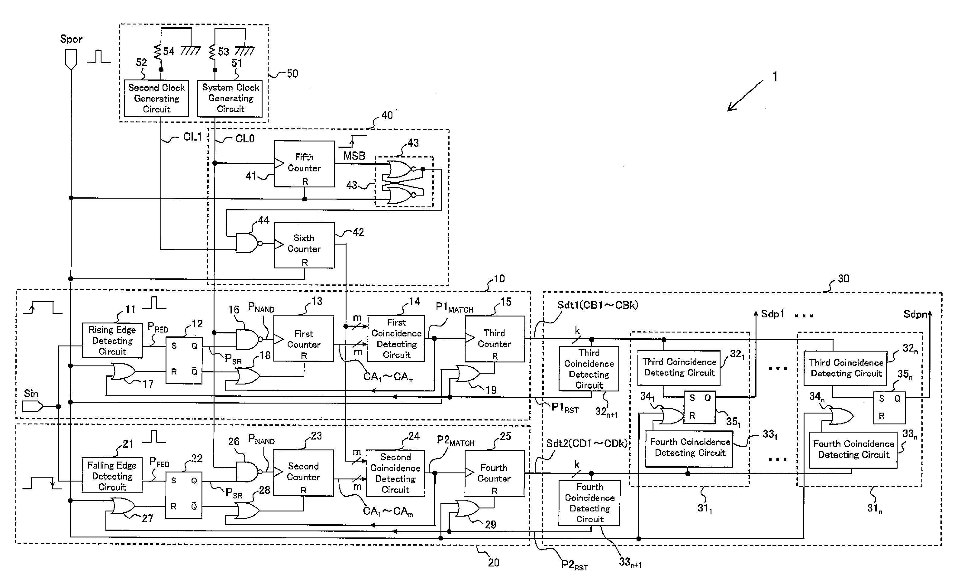
[0043]FIG. 1 is a logic circuit block diagram showing the circuit configuration of the pulse signal delay circuit according to the first embodiment of the present invention. The pulse signal delay circuit according to the present embodiment (hereinafter abbreviated to as “present delay circuit”) is formed of five circuit block sections. Concretely, as shown in FIG. 1, the present delay circuit 1 is configured by five circuit blocks: a first pulse edge delay circuit 10, a second pulse edge delay circuit 20, a delay pulse signal generating circuit 30, a delay counter value generating circuit 40 and a clock generating circuit 50.

[0044]The first pulse edge delay circuit 10 detects a rising edge of the PWM signal Sin being an input pulse signal, and generates a first delay timing signal Sdt1 for sequentially outputting the first edge detection delay timing, gained by delaying the detection timing of the rising edge by a preset delay time Δt a predetermined number of times (n) within one ...

second embodiment

[0066]Next, the LED drive circuit according to one embodiment of the present invention is described. The LED drive circuit according to the present embodiment (hereinafter abbreviated to as “present drive circuit”) is configured using the present delay circuit 1 according to the first embodiment. Accordingly, this circuit configuration is the same as that of the present delay circuit 1 shown in FIG. 1 and is configured by five circuit blocks: a first pulse edge delay circuit 10, a second pulse edge delay circuit 20, a delay pulse signal generating circuit 30, a delay counter value generating circuit 40 and a clock generating circuit 50. As shown in FIG. 5, the present drive circuit 2 is an LED drive circuit for driving an LED circuit 60, which is configured by connecting in parallel a plurality (n) of circuit units 64 (641 to 64n) gained by connecting in series an LED series circuit 62 gained by connecting a plurality of LEDs 61 in series in the same direction and a drive transistor...


PUM


Abstract

A pulse signal delay circuit comprises: a first pulse edge delay circuit for generating a first delay timing signal for sequentially outputting a first edge detection delay timing gained by detecting the rising edge of an input pulse signal and delaying the detection timing by a constant delay time a predetermined number of times; a second pulse edge delay circuit for generating a second delay timing signal for sequentially outputting a second edge detection delay timing gained by detecting the falling edge of the input pulse signal and delaying the detection timing by the delay time the number of times; and a delay pulse signal generating circuit for generating and outputting delay pulse signals rising and falling according to the first and second edge detection delay timings, respectively, from the first and second delay timing signals, the first and second edge detection delay timings delayed the same number of times.

Description

CROSS REFERENCE TO RELATED APPLICATION[0001]This Nonprovisional application claims priority under 35 U.S.C. §119(a) on Patent Application No. 2007-334623 filed in Japan on Dec. 26, 2007, the entire contents of which are hereby incorporated by reference.BACKGROUND OF THE INVENTION[0002]1. Field of the Invention[0003]The present invention relates to a pulse signal delay circuit which can be applied in an LED drive circuit and the like and generates a delay pulse signal by copying an input pulse signal with a delay of a predetermined delay time, as well as an LED drive circuit using the same.[0004]2. Description of the Related Art[0005]In an LED drive circuit and the like using a DC / DC converter technology, a smoothing condenser is charged by a booster circuit via Schottky diode and a constant voltage value is set. A current is supplied to a load connected parallel to the smoothing condenser from the booster circuit and its smoothing condenser. Recently, as the size of devices has been...

Claims


Application Information

Patent Timeline
Patent Type & Authority Applications(United States)
IPC IPC(8): H03H11/26H01L33/00H03K5/1532H03K17/78
CPCH05B33/0815Y02B20/346H05B33/0827H05B33/0818H05B45/46Y02B20/30H05B45/38
Inventor OISHI, YOSHIHIROFUJIWARA, MAKOTO
Owner SHARP KK
Why Eureka
Try Eureka