Display device and terminal unit using the same

a technology of display device and terminal unit, applied in the direction of optics, instruments, electrical apparatus, etc., can solve the problems of large contrast lowering, uneven gap between the pair of substrates, and high cost, so as to prevent the effect of display quality

Active Publication Date: 2009-07-02
NEC LCD TECH CORP
View PDF8 Cites 32 Cited by
  • Summary
  • Abstract
  • Description
  • Claims
  • Application Information

AI Technical Summary

Benefits of technology

[0029]A chief object of the present invention is to provide a display device that reduces the image quality degradations by suppressing the effect of the defective alignment regions caused by the spacers while minimizing the aperture ratio lowering, that prevents the image quality change dependent on the observation positions, and that avoids the problems arisen from the placement of the spacers in the two forms of the related-art three-dimensional LCD devices disclosed in the aforementioned Patent Document 2, and a terminal unit using the display device.
[0097]In a still further preferred embodiment of the display device according to the fourth aspect of the invention, two or more of the spacers are placed in each of the unit pixels of the first group and the unit pixels of the second group, wherein the spacers are shifted to each other along the direction perpendicular to the image separation axis of the optical image separation element in each of the unit pixels. In this embodiment, there is an advantage that it is easy to cope with the restriction as to the positions of the spacers to be placed.

Problems solved by technology

In this case, a disadvantage of large contrast lowering arises because some unevenness of alignment of the liquid crystal molecules occurs in the vicinities of the granular spacers placed on the pixels.
Moreover, when the viewer's side substrate of the LCD panel is thinned, there arises another disadvantage that the gap unevenness between the pair of substrates is likely to occur due to the distribution non-uniformity (i.e., randomness) of the granular spacers, and that this gap unevenness is likely to become large gradually due to the rigidity lowering of the substrates and / or the distortion release thereof.
Since the granular spacers may be moved within the substrate gap in the polishing process of the viewer's side substrate, there is a possibility that the granular spacers gathered at specific positions are recognized as display unevenness.
However, even with a high-definition LCD panel using the columnar spacers, there is a possibility that the regions of the alignment film hidden behind the columnar spacers are not sufficiently rubbed due to the pressing force insufficiency of the rubbing material in the rubbing process of the alignment film for giving the initial alignment to the liquid crystal molecules.
This causes a problem that the alignment of the liquid crystal molecules is defective in the regions hidden behind the columnar spacers.
Moreover, since the alignment direction of the liquid crystal molecules is distorted near the columnar spacers, a problem that the alignment of the liquid crystal molecules is defective may be arisen even if the rubbing process is not carried out.
The defective alignment regions of the liquid crystal molecule, which are formed by the columnar spacers in this way, will give rise to disadvantages (e.g., optical leakage), and as a result, these defective alignment regions will be a cause for various image quality degradations including contrast lowering.
For this reason, with a display device capable of displaying different images for a plurality of viewpoints, like a three-dimensional LCD device configured by combining a high-definition LCD panel including the aforementioned columnar spacers with an optical image separation element, there is a disadvantage that the image quality degradations (e.g., optical leakage) due to the aforementioned defective alignment regions will be recognized only at the specific observation positions (in other words, the said image quality degradations will change dependent on the observation positions).
Furthermore, since the images for the respective viewpoints are enlarged and displayed, the aforementioned defective alignment regions are likely to be recognized by the viewer.
As a result, there arises a problem that non-light-transmission regions (through which the light does not penetrate due to the existence of the columnar spacers) are generated at the front of the three-dimensional LCD device.
As a result, the non-light-transmission regions are generated at the front of the three-dimensional LCD device, which causes a problem that the regions where images are not seen are formed.
As a result, there arises a problem that the non-displayable regions where desired images are unable to be displayed may be formed.

Method used


Image

  • Display device and terminal unit using the same
  • Display device and terminal unit using the same
  • Display device and terminal unit using the same

Examples


first embodiment

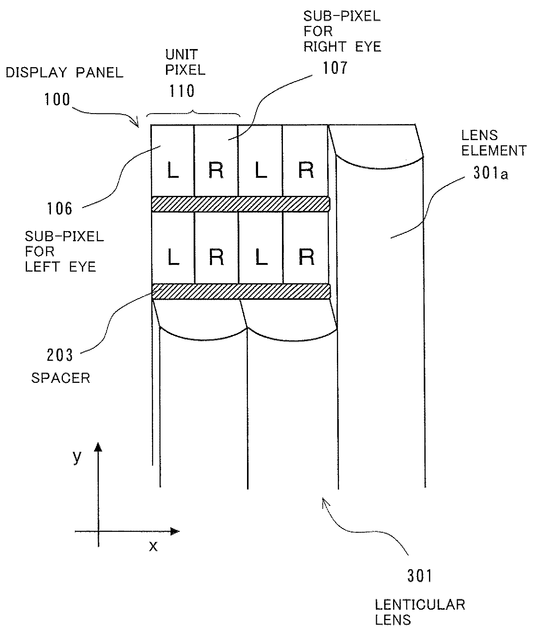
[0133]FIGS. 3 to 6 show a display device according to a first embodiment of the present invention.

[0134]As shown in FIG. 6, the display device according to the first embodiment comprises a display panel 100 and a lenticular lens 301.

[0135]The display panel 100, which has a structure of LCD panel, comprises a main substrate 101, an opposite substrate 201 bonded and unified with the main substrate 101 in such a away as to have a predetermined gap therebetween, and a liquid crystal layer 404 injected into the gap between the substrates 101 and 201. The gap between the substrates 101 and 201 (which may be simply termed the “substrate gap”) is kept approximately uniform over the whole surface of the panel 100 by spacers 203 arranged and fixed at predetermined positions between the substrate 101 and 201. Each of the spacers 203 is stripe-shaped.

[0136]As clearly shown in FIG. 4, the main substrate 101 comprises gate lines 103 extending along the horizontal direction of FIG. 4 (i.e., the x ...

second embodiment

[0164]FIGS. 11 and 12 show the pixel structure of the display panel 100A used in a display device according to a second embodiment of the present invention.

[0165]The display panel 100A according to the second embodiment is the same as the display panel 100 according to the aforementioned first embodiment except that the spacers 203, which are extended along the x direction in the form of stripes in the first embodiment, are divided into parts for the respective sub-pixels 106 and 107. In other words, the display panel 100A comprises the discontinuous or isolated spacers 203 in the respective sub-pixels 106 for the left eye and the respective sub-pixels 107 for the right eye, where these isolated spacers 203 are arranged along the x direction at the predetermined intervals. Accordingly, the explanation about the same structural components will be omitted here by attaching the same reference numerals as used in the first embodiment to these components.

[0166]It is apparent that the sam...

third embodiment

[0169]FIG. 14 shows the pixel structure of the display panel used in a display device according to a third embodiment of the present invention. FIGS. 15 to 18 show first to fourth variations of the structure of the display panel of FIG. 14, respectively.

[0170]With the structure of FIG. 14, the display panel comprises the unit pixels 110 each including two isolated spacers 203 and the unit pixels 110 including no spacers. The structure of each unit pixel 110 including the isolated spacers 203 is the same as that used in the aforementioned second embodiment shown in FIGS. 11 and 12. Specifically, one isolated spacer 203 is assigned to the sub-pixel 106 for the left eye of the unit pixel 110 and another isolated spacer 203 is assigned to the sub-pixel 107 for the right eye thereof.

[0171]The unit pixels 110 including the isolated spacers 203 are arranged along one column of the matrix (i.e., the y direction), which constitute the first pixel group. The unit pixels 110 including no space...


PUM


Abstract

A display device reduces the image quality degradations by suppressing the effect of the defective alignment regions caused by the spacers while minimizing the aperture ratio lowering, and prevents the image quality change dependent on the observation positions. The display device has a display panel and a lenticular lens. Each unit pixel of the display panel includes the sub-pixel for the left eye and the sub-pixel for the right eye. To keep the pair of substrates at a predetermined gap, spacers are arranged at predetermined positions in the gap. The spacers are stripe-shaped and extended along a direction perpendicular to the image separation axis of the lenticular lens. The spacers are equally overlapped with the sub-pixels for the left eye and those for the right eye. The spacers may be isolated for the respective unit pixels, or the first or second sub-pixels.

Description

BACKGROUND OF THE INVENTION[0001]1. Field of the Invention[0002]The present invention relates to a display device and a terminal unit using the same and more particularly, to a display device capable of displaying different images for a plurality of viewpoints and a terminal unit using the display device.[0003]2. Description of the Related Art[0004]In recent years, mounting Liquid Crystal Display (LCD) devices on small-sized electronic equipment such as projectors and portable telephones has been increasing rapidly to exploit the features of the LCD devices, i.e., low power consumption, reduced weight, and low profile. On the other hand, value-added products to be fabricated by adding some function or performance to the LCD device have also been developed, an example of which is the three-dimensional LCD device capable of displaying three-dimensional images using an optical element that separates images for different viewpoints (i.e., an optical image separation element). With the t...

Claims


Application Information

Patent Timeline
Patent Type & Authority Applications(United States)
IPC IPC(8): G02B27/22G02B30/27
CPCG02B27/2214G02F1/13394H04N13/0422H04N13/0406H04N13/0404H04N13/305H04N13/324H04N13/307G02B30/27
Inventor HIROYA, TSUTOMUUEHARA, SHINICHISHIGEMURA, KOJI
Owner NEC LCD TECH CORP
Why Eureka
Try Eureka