Peak Power Reduction Methods in Distributed Charge Pump Systems

a charge pump and peak power technology, applied in the direction of generating/distributing signals, pulse techniques, instruments, etc., can solve the problems of high cost and inefficiency of excess power usage, heat management problems, and special problems, and achieve the effect of optimizing voltage regulation and reducing peak power usag

Inactive Publication Date: 2009-07-09
IBM CORP
View PDF11 Cites 58 Cited by
  • Summary
  • Abstract
  • Description
  • Claims
  • Application Information

AI Technical Summary

Benefits of technology

[0013]It is another object of the present invention to provide such a system which does not entail an excessive number of delay stages but still reduces peak power usage in a distributed charge pump system, particularly one utilizing switched-capacitor charge pumps.

Problems solved by technology

Excess power usage is not only costly and inefficient, but also leads to heat management problems.
These problems are particularly pronounced in computer systems having large amounts of memory.
However, DRAM can be more power intensive in circuit blocks for active power supply generation and refresh.
DRAM can consume a significant portion of a system's overall power.
Power management has become even more challenging with the advent of new memory technologies like embedded DRAM (eDRAM).
While peak current is not particularly troublesome for a single charge pump, it can become excessive in larger systems having multiple charge pumps.
If these pumps all run on the same clock signal, charge pump peak power and transient current supply current is multiplied by a factor of 96, which would significantly burden the system power budget and heat sink cost.
Methods have been devised which address peak power consumption in voltage supplies for integrated circuits, but these methods still have various disadvantages.
This approach does not work well in high performance systems with large embedded DRAM since instantaneous switching power can still be many times higher.
This multiplicity of blocks is inefficient for large on-board designs, and also presents problems with variability and the power burden on the clock network itself.
Phase offset by delay stages does not work well for newer technologies (with FO4 delays in the neighborhood of 10 picoseconds) since it may take up to 250 such delay stages to move just one clock edge of a 100 MHz clock by 25% of its period.
In particular, supply generation for eDRAM word lines in server class applications entails special challenges because of the stringent power, performance, cell retention, variability, and distribution requirements.

Method used


Image

  • Peak Power Reduction Methods in Distributed Charge Pump Systems
  • Peak Power Reduction Methods in Distributed Charge Pump Systems
  • Peak Power Reduction Methods in Distributed Charge Pump Systems

Examples


Embodiment Construction

)

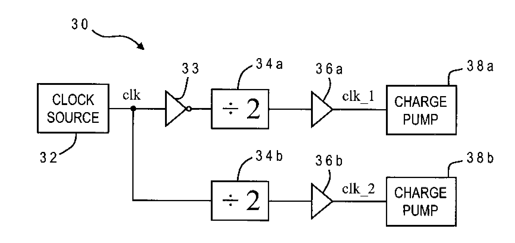
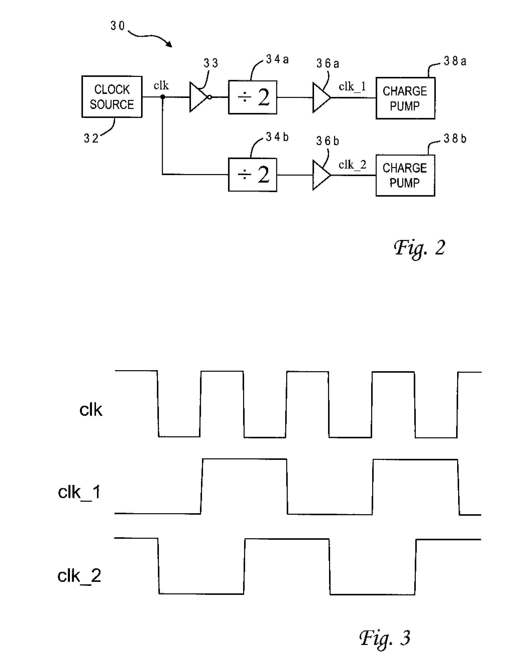
[0028]With reference now to the figures, and in particular with reference to FIG. 2, there is depicted a simplified embodiment 30 of a distributed charge pump system constructed in accordance with the present invention. Distributed charge pump system 30 is generally comprised of a clock source 32, a delay element 33 which receives the clock signal “clk” from clock source 32, a first frequency divider 34a which receives a delayed clock signal from delay element 33, a second frequency divider 34b which receives the undelayed clock signal from clock source 32, two buffers 36a, 36b respectively connected to the outputs of frequency dividers 34a, 34b, and two charge pumps 38a, 38b driven by respective clock signals “clk_1” and “clk_2” from buffers 36a, 36b. Clock source 32 may for example be a phase-lock loop circuit utilizing an oscillator. Delay element 33 is an inverter in this embodiment but may comprise other circuit structures which exhibit a known delay in conveying the clock sig...


PUM


Abstract

A distributed charge pump system uses a delay element and frequency dividers to generate out of phase pump clock signals that drive different charge pumps, to offset peak current clock edges for each charge pump and thereby reduce overall peak power. Clock signal division and phase offset may be extended to multiple levels for further smoothing of the pump clock signal transitions. A dual frequency divider may be used which receives the clock signal and its complement, and generates two divided signals that are 90° out of phase. In an illustrative embodiment the clock generator comprises a variable-frequency clock source, and a voltage regulator senses an output voltage of the charge pumps, generates a reference voltage based on a currently selected frequency of the variable-frequency clock source, and temporarily disables the charge pumps (by turning off local pump clocks) when the output voltage is greater than the reference voltage.

Description

BACKGROUND OF THE INVENTION[0001]1. Field of the Invention[0002]The present invention generally relates to voltage supplies for integrated circuits, and more particularly to distributed charge pump systems used to power electronic memory structures such as dynamic random-access memory (DRAM).[0003]2. Description of the Related Art[0004]Power management has become a dominant concern in the development of data processing systems. Excess power usage is not only costly and inefficient, but also leads to heat management problems. These problems are particularly pronounced in computer systems having large amounts of memory. State of the art computer systems typically use dynamic random-access memory (DRAM) which is preferable over other memory structures such as static random-access memory (SRAM) because DRAM is more dense. However, DRAM can be more power intensive in circuit blocks for active power supply generation and refresh. SRAM uses a flip-flop memory cell but DRAM uses a capacitor...

Claims


Application Information

Patent Timeline
Patent Type & Authority Applications(United States)
IPC IPC(8): H03K21/00H03L7/06G06F1/04
CPCH02M3/073H03L5/00H02M2003/077H02M3/077
Inventor GEBARA, FADI H.KUANG, JENTE B.MATHEWS, ABRAHAM
Owner IBM CORP
Why Eureka
Try Eureka