Pulse generation circuit and modulator
- Summary
- Abstract
- Description
- Claims
- Application Information
AI Technical Summary
Benefits of technology
Problems solved by technology
Method used
Image
Examples
first embodiment
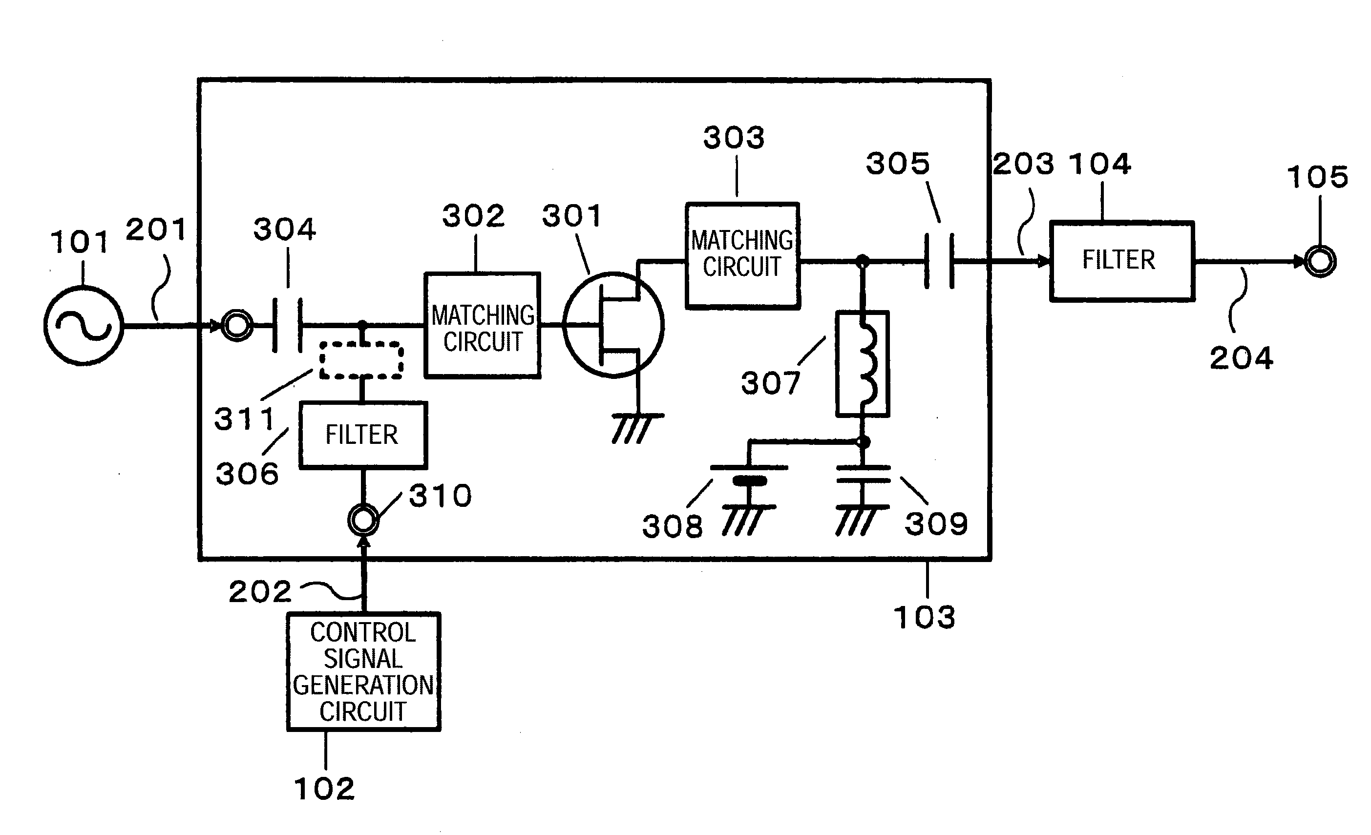
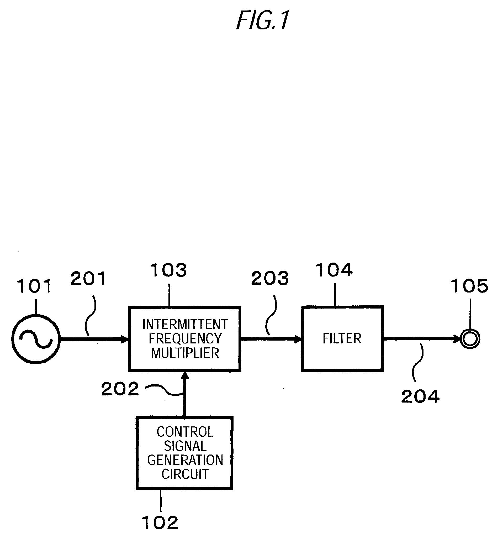
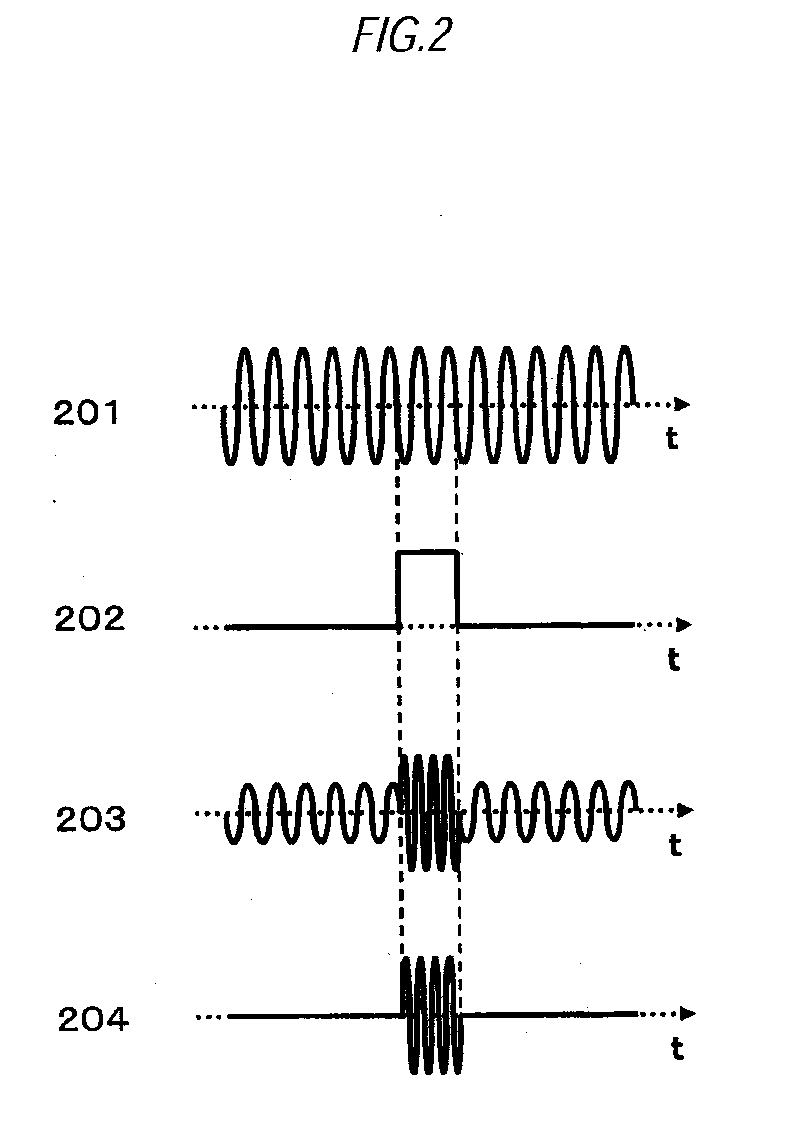
[0159]FIG. 1 is a block diagram of a short pulse generation circuit in a first embodiment of the invention. The short pulse generation circuit shown in FIG. 1 includes an oscillator 101, a control signal generation circuit 102, an intermittent frequency multiplier 103, a filter 104, and an output terminal 105. The intermittent frequency multiplier is a circuit for directly controlling a frequency multiplier by a control signal and intermittently operating the circuit. The oscillator 101 and the intermittent frequency multiplier 103 are active circuits implemented as active elements.
[0160]In the description to follow, it is assumed that the active element is an FET (Field-Effect Transistor). Although the multiple number of the intermittent frequency multiplier is n (n: Positive integer), in the description to follow, it is assumed that the desired frequency of an output signal is f0, that the frequency of an output signal of the oscillator is f0 / 2, and that the intermittent frequency...
second embodiment
[0211]FIG. 9 is a block diagram to show the configuration of a short pulse generation circuit in a second embodiment of the invention. The short pulse generation circuit differs from that in the first embodiment described above in that an intermittent differential frequency multiplier 902 is used in place of the intermittent frequency multiplier 103, that a differential oscillator 901 is used in place of the oscillator 101 at the preceding stage, that the filter 104 is not required, and that a waveform combining circuit 903 is used.
[0212]The circuit configuration is of differential type and the waveform combining circuit 903 is provided, so that the short pulse generation circuit for suppressing a spurious component without any filter and generating a short pulse signal having a high On / Off ratio and high CN can be realized with low power consumption.
[0213]FIG. 10 is a timing chart to show change in a control signal and input / output signals in the short pulse generation circuit show...
third embodiment
[0227]FIG. 13 is a block diagram to show the configuration of a short pulse generation circuit in a third embodiment of the invention. The short pulse generation circuit differs from that in the first embodiment described above in that the oscillator 101 is replaced with an intermittent oscillator 1301, that the control signal generation circuit 102 is replaced with a control signal generation circuit 1302, and that a control signal 1401 output from the control signal generation circuit 1302 is input to the intermittent oscillator 1301.
[0228]The oscillator is intermittently operated like an intermittent frequency multiplier, whereby lower power consumption and a higher On / Off ratio can be realized. Here, it is assumed that a short pulse signal output from the intermittent oscillator 1301 and a control signal for controlling an intermittent frequency multiplier 103 differ in pulse width and the former has a longer pulse width than the latter.
[0229]FIG. 14 is a timing chart to show ch...
PUM
 Abstract
Description
Claims
Application Information


