Assembled circuit and electronic component

a technology of assembled circuits and electronic components, applied in the direction of final product manufacturing, sustainable manufacturing/processing, semiconductor/solid-state device details, etc., can solve the problems of pol dc to dc converters that all suffer from oversized overall volume and low power density, and achieve the effect of improving the power density of dc to dc converters, shrinking an overall size, and increasing integration

Active Publication Date: 2009-07-09
DELTA ELECTRONICS INC
View PDF19 Cites 57 Cited by
  • Summary
  • Abstract
  • Description
  • Claims
  • Application Information

AI Technical Summary

Benefits of technology

[0012]One objective of this invention is to provide an assembled circuit for use with a carrier. The assembled circuit is applied to e.g. a DC to DC converter to increase the integration, shrink an overall size and improve a power density of the DC TO DC-converter. The DC to DC converter is e.g. a buck DC TO DC converter, and particularly a point of load (POL) DC to DC converter.

Problems solved by technology

These inevitably increase the volume of the POL DC to DC converter 2 and further lowers the overall power density thereof.
In summary, the conventional POL DC to DC converters all suffer from the oversized overall volume and the low power density due to the pin arrangement in the conventional package.

Method used


Image

  • Assembled circuit and electronic component
  • Assembled circuit and electronic component
  • Assembled circuit and electronic component

Examples


first embodiment

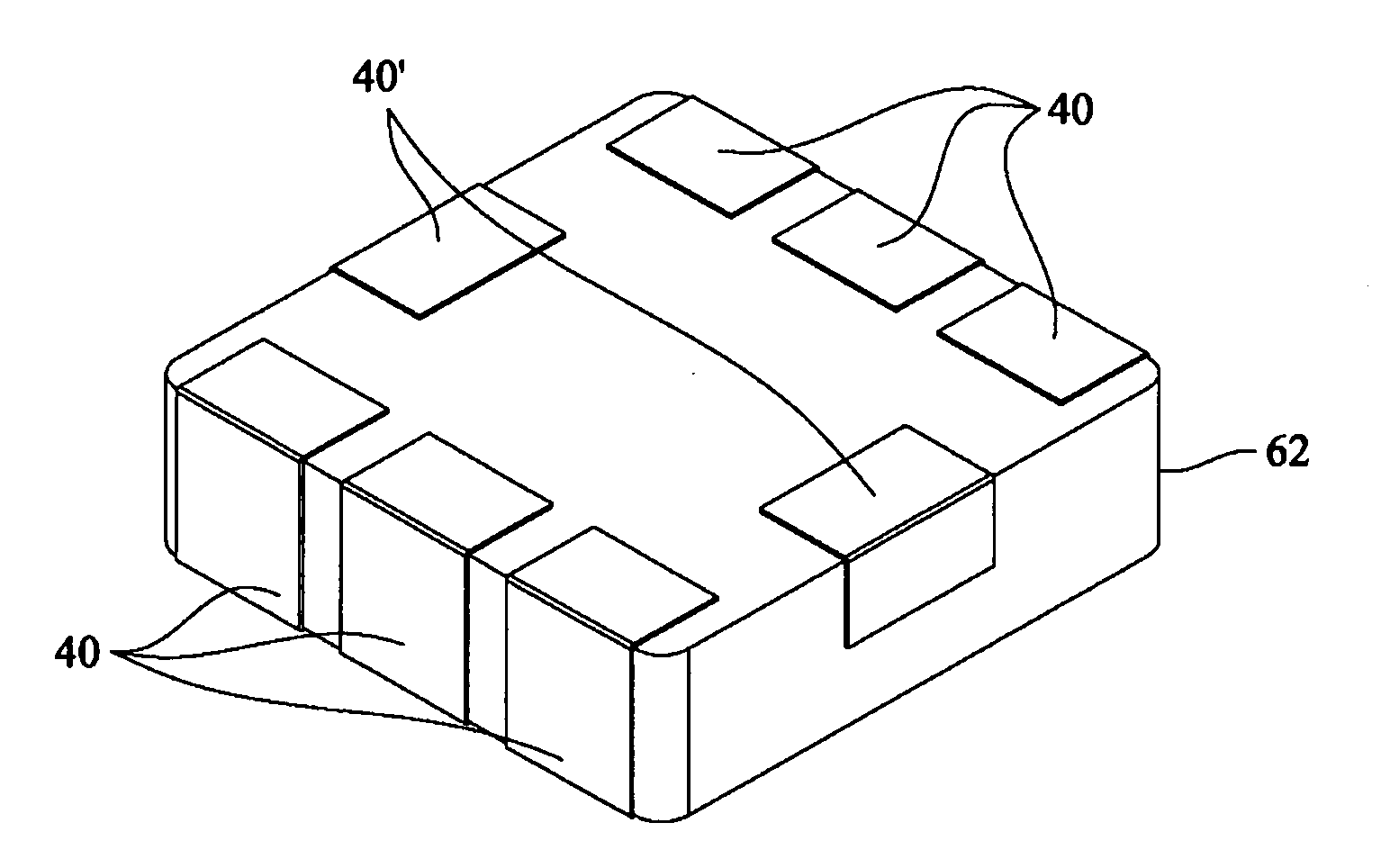
[0057]To effectively improve the power density and shrink the overall dimensions of an electronic apparatus, particularly a power converter, this invention provides a novel pin scheme adapted to be widely used in a variety of common electronic apparatuses. Referring to FIGS. 4A, 4C and 4B, 4D, top views and bottom views of an inductive component 62 in accordance with this invention are illustrated respectively therein. More specifically, the inductive component 62 may be an inductor, and in practical application, may be a co-fired magnetic material inductor or a wire wound compressed inductor. It should be noted that, the inductive component 62 in this embodiment is only for purpose of illustration, and in practice, the technology disclosed in this invention may be applied to other electronic component such as a field-effect transistor (FET).

[0058]As one of the characteristics of this invention, an outer surface of the inductive component 62 is wrapped with a first conductive layer ...

third embodiment

[0073]FIGS. 11A to 11G illustrate this invention, which also relates to an assembled circuit applied to a DC to DC converter, and particularly a POL DC to DC converter. FIGS. 11A and 11B illustrate a top view and a bottom view of the POL DC to DC converter 110 respectively. The POL DC to DC converter 110 adopts an inductor made of a co-fired magnetic material as a substrate. The POL DC to DC converter 110 comprises an inductive component, a first conductive layer 112, two second electronic components, a fourth electronic component and an inductance coil 116. In this embodiment, the inductive component is formed by stacking a number of co-fired magnetic material substrates 111 together, the second electronic components are capacitors 114, and the fourth electronic component is an integrated circuit (IC) 115 integrating e.g. an FET (particularly an MOSFET) and a control chip together. As previously described, the first conductive layer 112 comprises a connecting conductor and a pin co...

fourth embodiment

[0076]FIGS. 12A to 12D illustrate this invention, which also relates to an assembled circuit applied to e.g. a DC to DC converter, and particularly a POL DC to DC converter 120. FIGS. 12A and 12B illustrate a top view and a bottom view respectively of the POL DC to DC converter 120 where an inductance coil 127 is compressed in a magnetic material substrate 125. The POL DC to DC converter 120 comprises a fourth electronic component, two second electronic components, a first conductive layer 123, and an inductive component. The fourth electronic component is an integrated circuit (IC) 121 having e.g. an FET (particularly an MOSFET) and a control chip integrated therein, the two second electronic components are both capacitors 122, and the inductive component comprises the magnetic material substrate 125 and the inductance coil 127 described above. As previously described, the first conductive layer 123 comprises a connecting conductor having four pins 124 and a pin conductor having tw...


PUM


Abstract

An assembled circuit comprising an inductive component, a connecting conductor, and a first electronic component is disclosed. The connecting conductor is adapted to wrap a first surface of the inductive component. The first electronic component stacks on the inductive component. The assembled circuit is electrically connected to the carrier via the connecting conductor.

Description

CROSS-REFERENCE TO RELATED APPLICATION(S)[0001]This application claims priority to Taiwan Patent Application No. 097100160 filed on 03 Jan. 2008, the disclosure of which is incorporated herein by reference in its entirety.BACKGROUND OF THE INVENTION[0002]1. Field of the Invention[0003]The present invention relates to an electronic component and an assembled circuit using the same; and more particularly, the present invention relates to an electronic component and an assembled circuit that can improve power density of a power supply as a whole by reducing an overall size of the electronic component.[0004]2. Descriptions of the Related Art[0005]Nowadays with the development of the power supply technologies, requirements on the power density and the size of a power supply are more and more critical. There exists a variety of methods for increasing the power density of a power supply, among which a popular method is to increase the power density of a power supply by altering some electr...

Claims


Application Information

Patent Timeline
Patent Type & Authority Applications(United States)
IPC IPC(8): H05K7/00
CPCH01F17/0033H01F2017/048H01L2924/13055H01L2924/13091H01L2924/19105H01L2924/0002H01L2224/16225H02M3/00H05K1/141H05K1/145H05K3/3442H05K2201/1003H05K2201/10166H05K2201/1053H05K2201/10636H01F17/0013H05K7/026H01L2924/00Y02P70/50H02M3/003H01F27/2804H01F27/29
Inventor ZENG, JIAN-HONGYANG, WEIHONG, SHOU-YUYING, JIAN-PING
Owner DELTA ELECTRONICS INC
Why Eureka
Try Eureka