Display substrate having quantum well for improved electron mobility and display device including the same

a display substrate and electron mobility technology, applied in semiconductor devices, instruments, optics, etc., can solve the problems of relatively low electron mobility of amorphous silicon and problems with operational reliability, and achieve the effect of superior operational characteristics

a display substrate and electron mobility technology, applied in semiconductor devices, instruments, optics, etc., can solve the problems of relatively low electron mobility of amorphous silicon and problems with operational reliability, and achieve the effect of superior operational characteristics

US20090180045A1Active Publication Date: 2009-07-16SAMSUNG DISPLAY CO LTD

Image

  • Display substrate having quantum well for improved electron mobility and display device including the same
  • Display substrate having quantum well for improved electron mobility and display device including the same
  • Display substrate having quantum well for improved electron mobility and display device including the same

Examples


Embodiment Construction

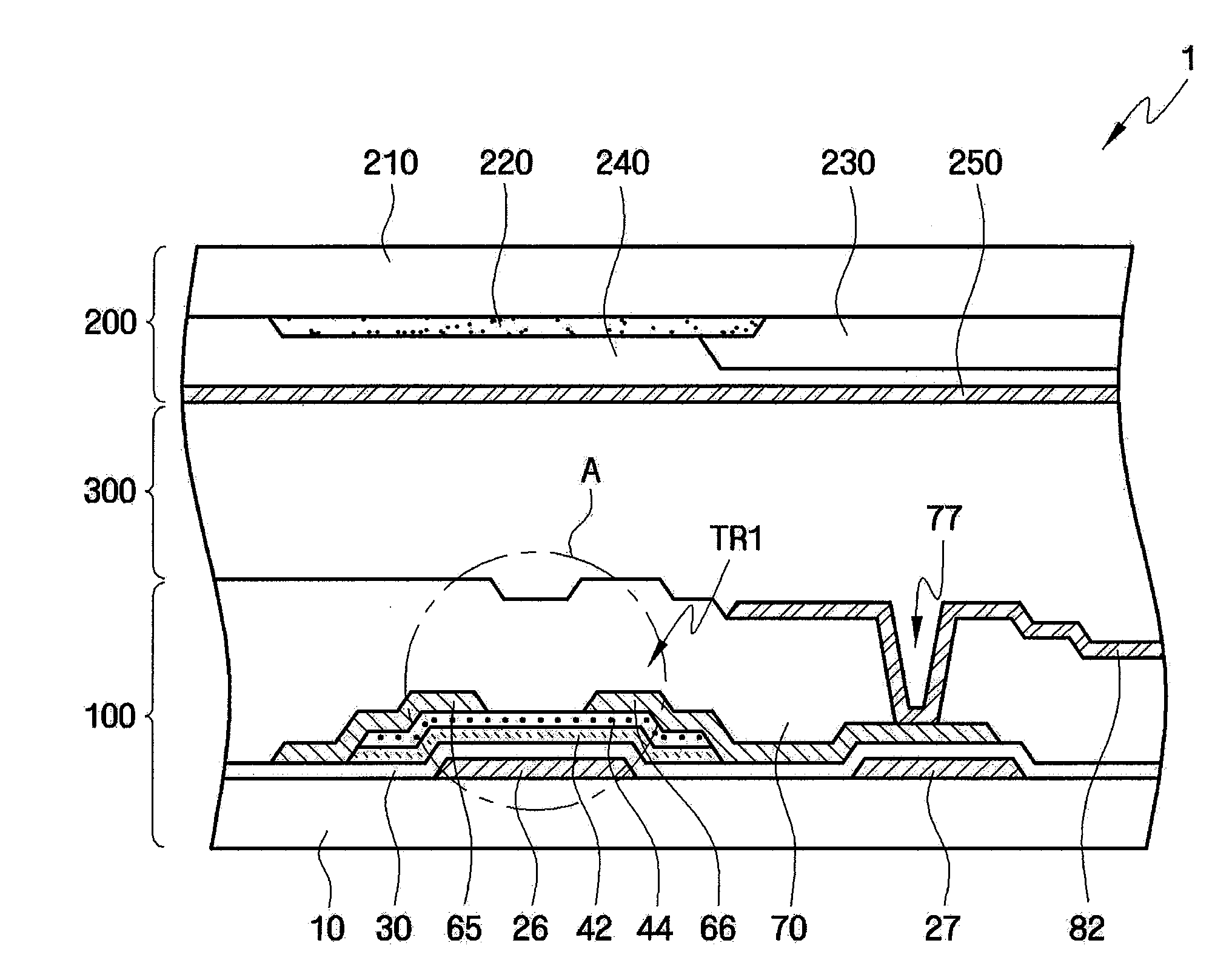
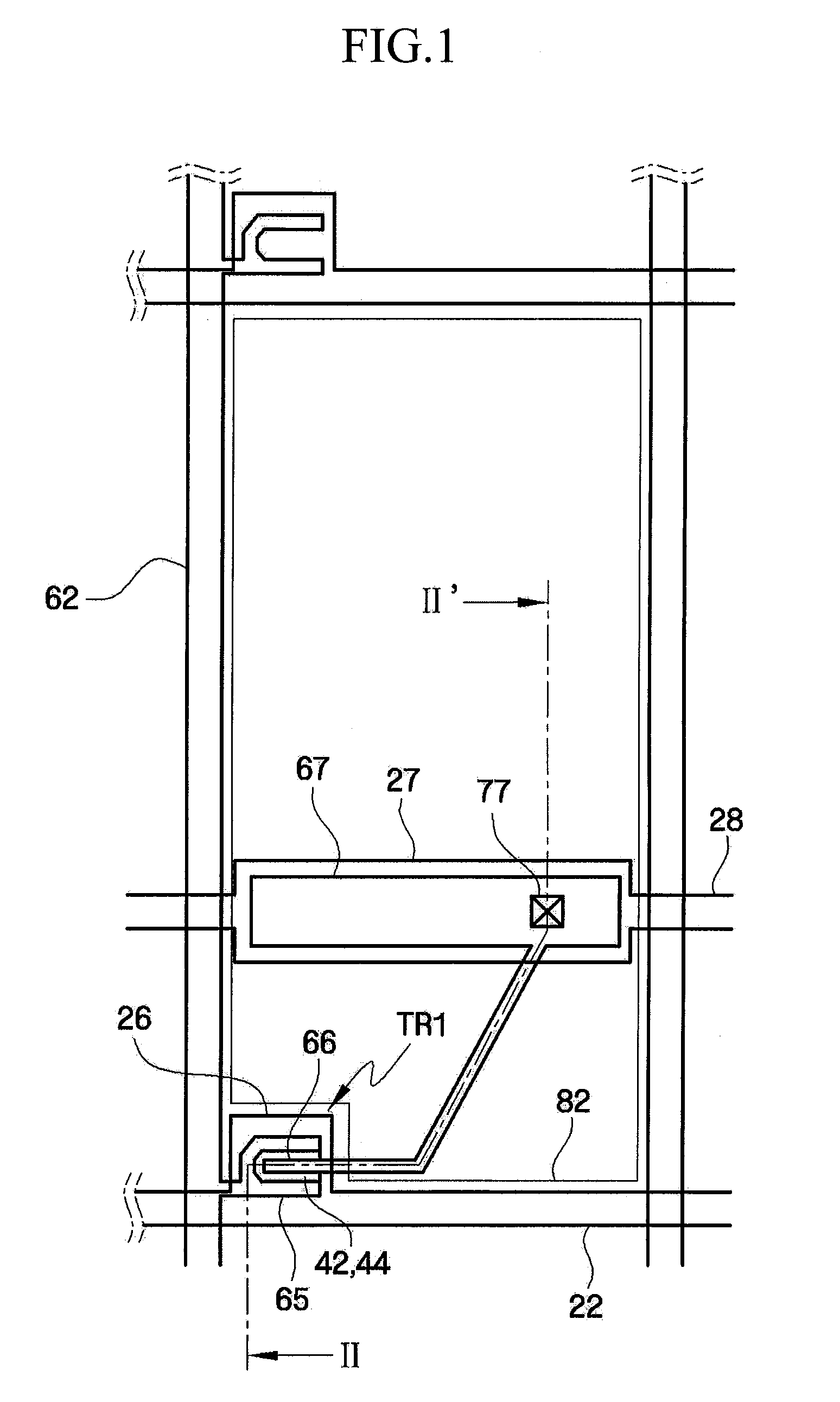
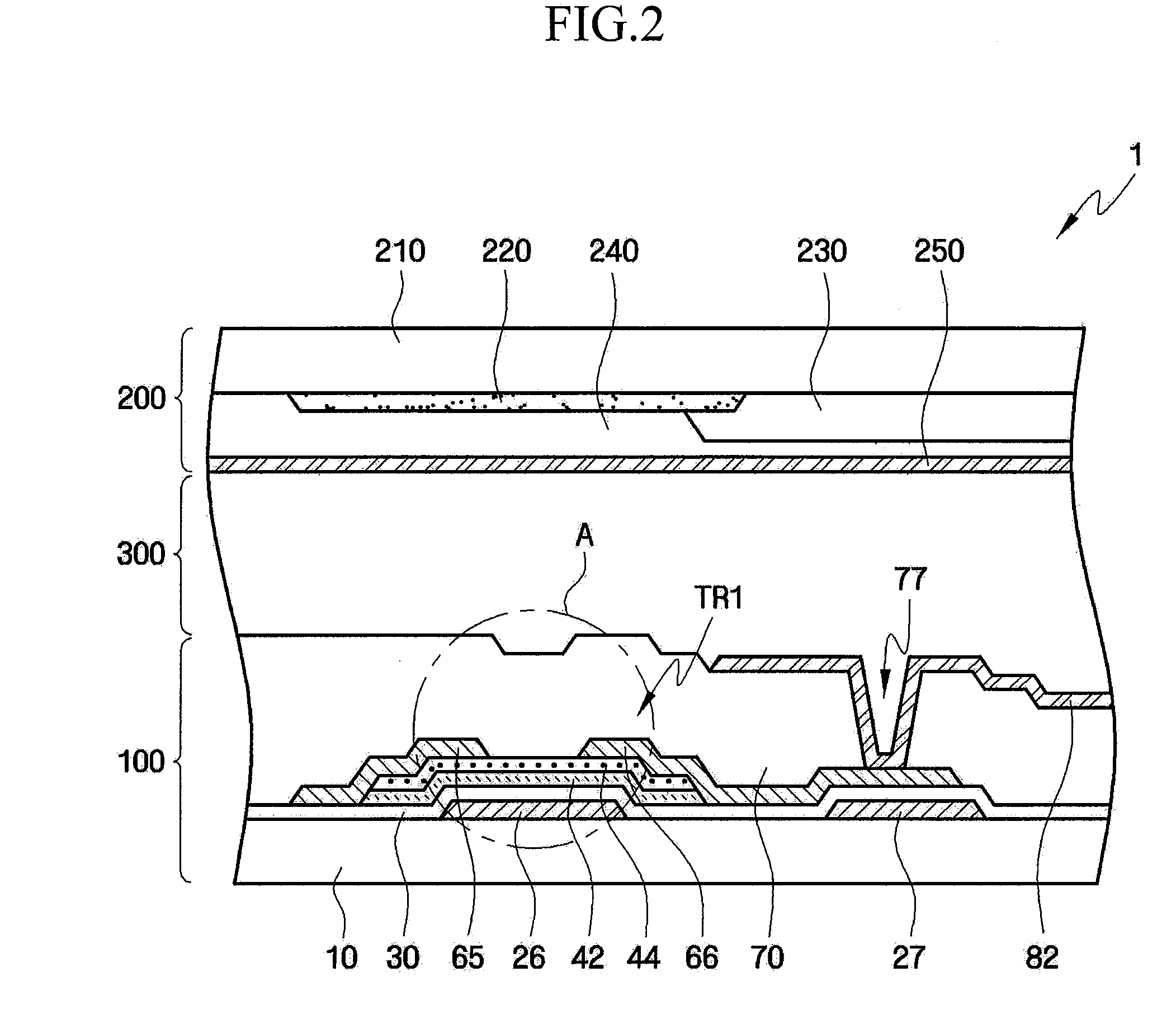
[0022]Advantages and features of the present invention and methods of accomplishing the same may be understood more readily by reference to the following detailed description of exemplary embodiments and the accompanying drawings. The present invention may, however, be embodied in many different forms and should not be construed as being limited to the embodiments set forth herein. Rather, these embodiments are provided so that this disclosure will be thorough and complete and will fully convey the concept of the invention to those skilled in the art. Accordingly, the present invention will only be defined by the appended claims. In some embodiments, well-known processing processes, well-known structures and well-known technologies will not be specifically described in order to avoid ambiguous interpretation of the present invention. Like reference numerals refer to like elements throughout the specification.

[0023]It will be understood that when an element or layer is referred to as...


PUM

PropertyMeasurementUnit
gate voltageaaaaaaaaaa
gate voltage Vgaaaaaaaaaa

Abstract

Provided are a display substrate and a display device including the same. The display substrate includes: gate wiring; a first semiconductor pattern formed on the gate wiring and having a first energy bandgap; a second semiconductor pattern formed on the first semiconductor pattern and having a second energy bandgap which is greater than the first energy bandgap; data wiring formed on the first semiconductor pattern; and a pixel electrode electrically connected to the data wiring. Because the second energy bandgap is larger than the first energy bandgap, a quantum well is formed in the first semiconductor pattern, enhancing electron mobility therein.

Description

[0001]This application claims priority from Korean Patent Application No. 10-2008-0004464 filed on Jan. 15, 2008 in the Korean Intellectual Property Office, the disclosure of which is incorporated herein by reference in its entirety.BACKGROUND OF THE INVENTION[0002]1. Field of the Invention[0003]The present invention relates to a display substrate and a display device including the same. More particularly, the present invention relates to display substrates having quantum wells for improved electron mobility, and display devices including the same.[0004]2. Description of the Related Art[0005]Continuous efforts are being made to improve display devices by increasing display size and quality. In particular, efforts are being made to improve the electrical characteristics of thin-film transistors (TFTs) that are commonly used to drive liquid crystal displays (LCDs).[0006]Conventional TFTs often employ a channel structure, formed with the assistance of a hydrogenated amorphous silicon (...

Claims


Application Information

Patent Timeline
16 Jul 2009
Publication
US20090180045A1
IPC
G02F1/1368; H01L27/08; H01L29/02
CPC
G02F1/1368; G02F2202/108; H01L27/1255; H01L29/7869; H01L27/1225; G02F1/136
Inventors
YOON, KAP-SOO; YANG, SUNG-HOON