Method for fabricating graphene transistors on a silicon or soi substrate

a graphene transistor and silicon or soi technology, applied in the field of semiconductor graphene transistor construction, can solve the problems of reducing the production efficiency of such devices, requiring significant man hours, and putting the current technology to its limits

Active Publication Date: 2009-07-16
TEXAS INSTR INC
View PDF12 Cites 112 Cited by
  • Summary
  • Abstract
  • Description
  • Claims
  • Application Information

AI Technical Summary

Benefits of technology

[0006]The following presents a simplified summary of the invention in order to provide a basic understanding of some aspects of the invention. This summary is not an extensive overview of the invention. It is intended neither to identify key or critical elements of the invention nor to delineate the scope of the invention. Rather, its primary purpose is merely to present one or more concepts of the invention in a simplified form as a prelude to the more detailed description that is presented later.

Problems solved by technology

These trends are pushing the current technology to its limits.
For example, significant man hours may be required to design such scaled down transistor devices, the equipment necessary to produce such devices may be expensive and / or processes related to producing such devices may have to be very tightly controlled and / or be operated under very specific conditions, etc.
Accordingly, it can be appreciated that there is significant costs associated with exercising quality control over semiconductor fabrication, including, costs associated with discarding defective units, wasting raw materials and / or man hours, for example.
Additionally, since the units are more tightly packed on the wafer, more units are lost when some or all of a wafer is defective and thus has to be discarded.
However, semiconductor devices utilizing graphene are currently difficult to construct.

Method used


Image

  • Method for fabricating graphene transistors on a silicon or soi substrate
  • Method for fabricating graphene transistors on a silicon or soi substrate
  • Method for fabricating graphene transistors on a silicon or soi substrate

Examples


Embodiment Construction

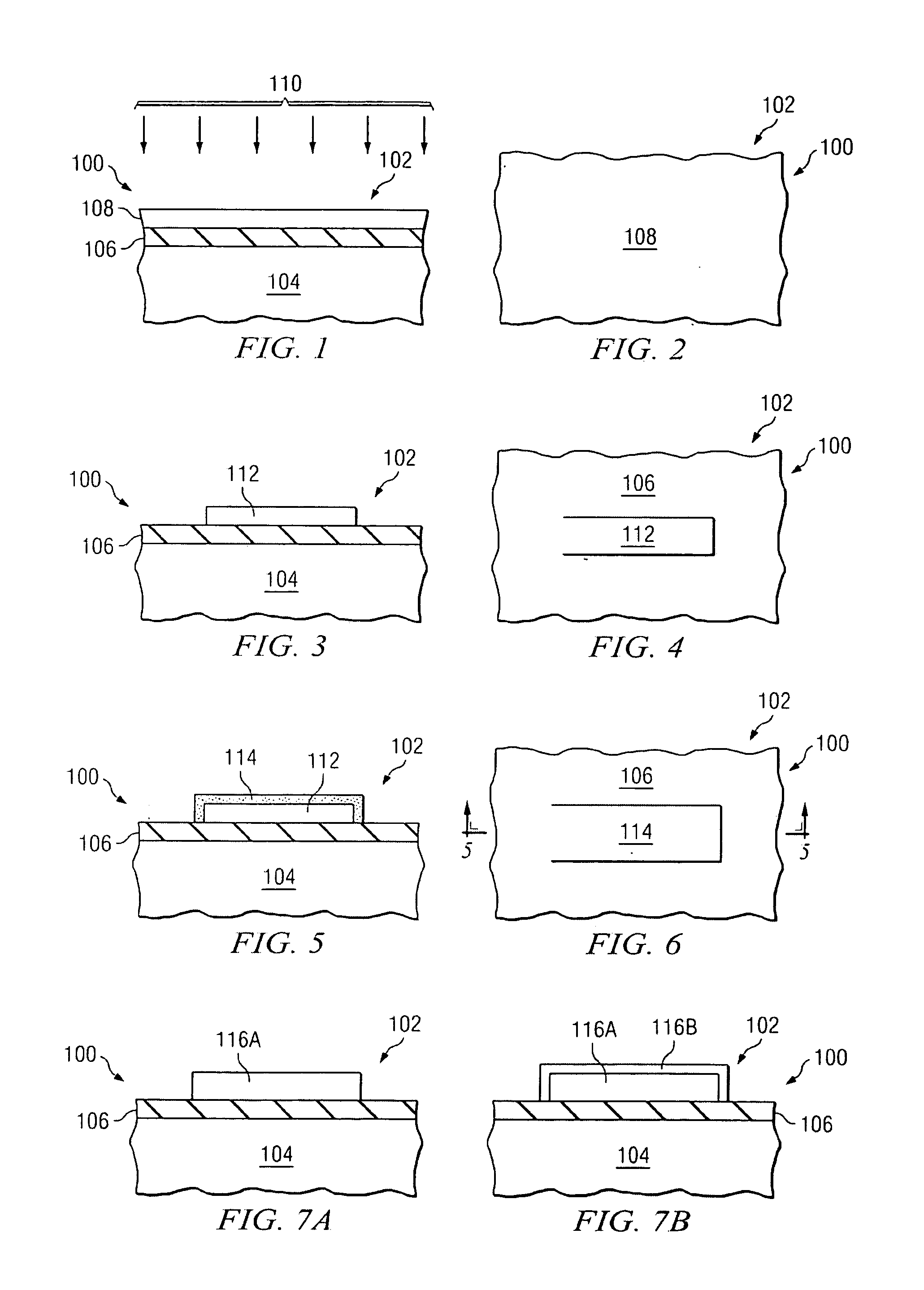
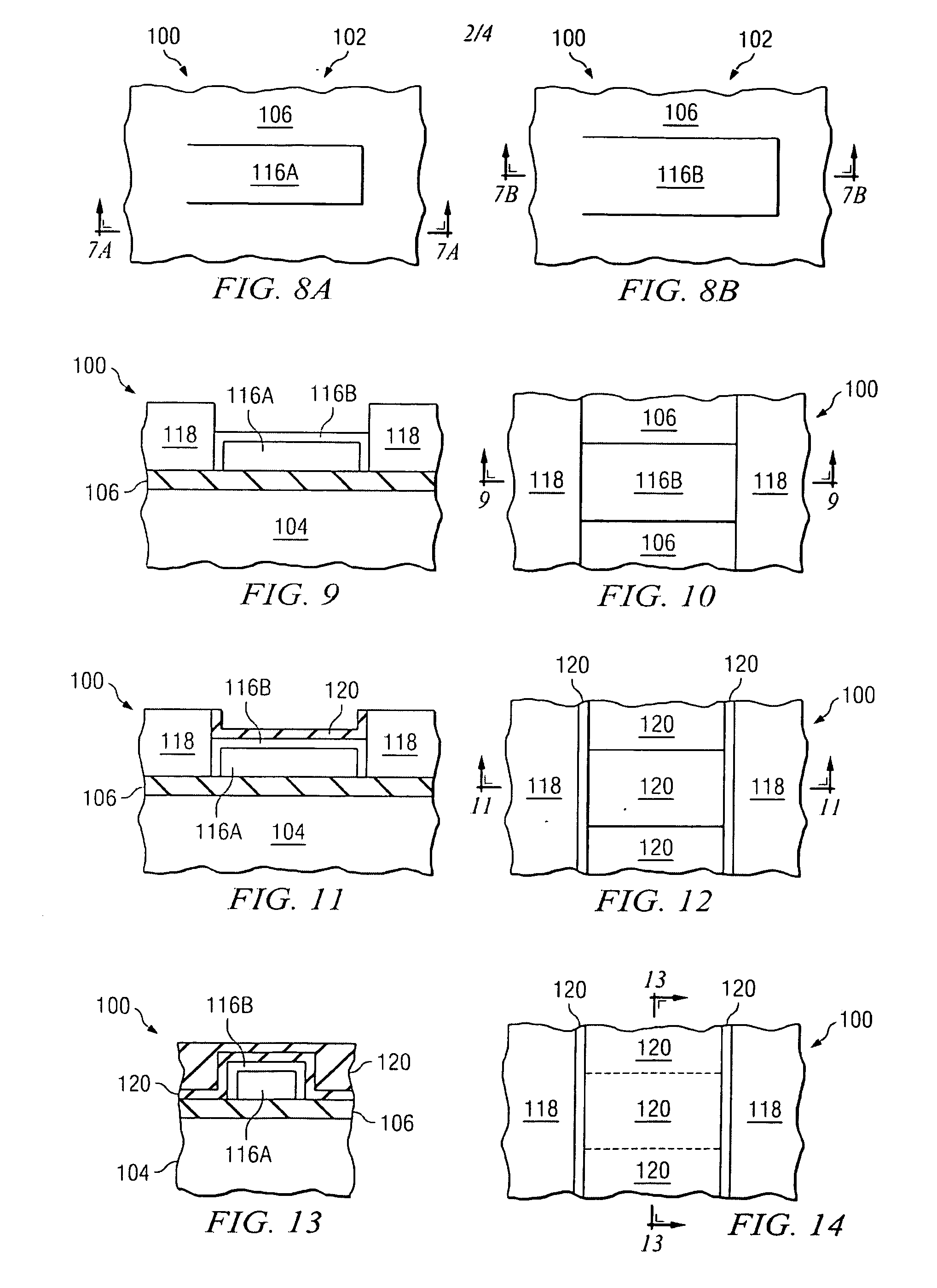
[0019]The description herein is made with reference to the drawings, wherein like reference numerals are generally utilized to refer to like elements throughout, and wherein the various structures are not necessarily drawn to scale. In the following description, for purposes of explanation, numerous specific details are set forth in order to provide a thorough understanding. It may be evident, however, to one skilled in the art, that one or more aspects described herein may be practiced with a lesser degree of these specific details. In other instances, known structures and devices are shown in block diagram form to facilitate a thorough understanding.

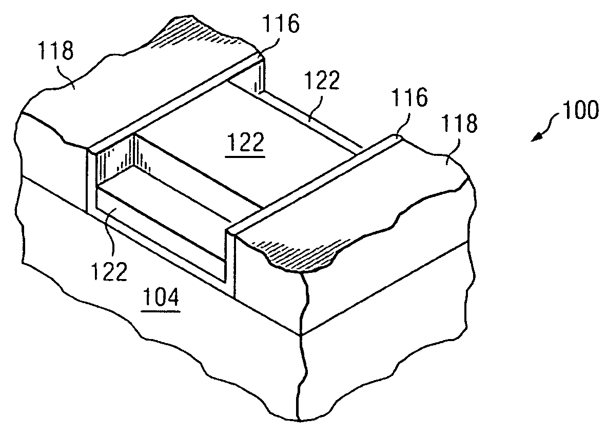
[0020]According to at least one embodiment of the present invention, a standard workpiece / wafer can be utilized that comprises a silicon-on-insulator (SOI) substrate. However a single crystal silicon substrate, a Poly-Si, or other substrate composites can be utilized as well. Such substrates are commercially obtainable and are fabricat...


PUM

PropertyMeasurementUnit
thicknessaaaaaaaaaa
melting pointaaaaaaaaaa
temperaturesaaaaaaaaaa

Abstract

A method of fabricating graphene transistors, comprising providing an SOI substrate, performing an optional threshold implant on the SOI substrate, forming an upper silicon layer mesa island, carbonizing the silicon layer into SiC utilizing a gaseous source, converting the SiC into graphene, forming source/drain regions on opposite longitudinal ends of the graphene, forming gate oxide between the source/drain regions on the graphene, forming gate material over the gate oxide, creating a transistor edge, depositing dielectric onto the transistor edge and performing back end processing.

Description

FIELD OF INVENTION[0001]The present invention relates generally to semiconductor processing, and more particularly to methods for constructing semiconductor graphene transistors on silicon, SOI or other composite silicon substrates.BACKGROUND OF THE INVENTION[0002]Several trends presently exist in the semiconductor and electronics industry. Devices are continually being made smaller, faster and requiring less power. One reason for these trends is that personal devices are being fabricated that are smaller and more portable, thereby relying on batteries as their primary supply. For example, cellular phones, personal computing devices, and personal sound systems are devices that are in great demand in the consumer market. In addition to being smaller and more portable, personal devices are also requiring increased memory, more computational power and speed. In light of these trends, there is an ever increasing demand in the industry for smaller and faster transistors used to provide t...

Claims


Application Information

Patent Timeline
Patent Type & Authority Applications(United States)
IPC IPC(8): H01L21/336
CPCH01L29/1606H01L29/78684H01L29/7781H01L29/66742
Inventor PARIKH, ASHESHMARSHALL, ANDREW
Owner TEXAS INSTR INC
Why Eureka
Try Eureka