Semiconductor device including semiconductor chips with different thickness

a semiconductor chip and semiconductor technology, applied in the field of semiconductor devices, can solve the problems of warpage, difficulty in reducing the area of a semiconductor chip, and difficulty in improving the mechanical reliability of the semiconductor device, and achieve the effect of relieved warpage of the semiconductor device due to heat during us

Active Publication Date: 2009-07-23
LONGITUDE LICENSING LTD
View PDF1 Cites 9 Cited by
  • Summary
  • Abstract
  • Description
  • Claims
  • Application Information

AI Technical Summary

Benefits of technology

[0018]According to this configuration, the warpage of the semiconductor devices due to heat during use can be relieved.

Problems solved by technology

However, due to factors, such as the larger scale, the complexity of peripheral circuits, and the difficulty of shortening of manufacturing process, it is difficult to decrease the area of a semiconductor chip.
The restriction on the positions of the connection terminals according to this standard is one of the factors that account for the difficulty in improving the mechanical reliability of the semiconductor device.
In the stacked-type semiconductor device, due to a difference in the linear expansion coefficient between the semiconductor chip and the wiring board, warpage is caused by heat during use.
However, in the chip-stacked-type semiconductor device described in Japanese Patent Laid-Open No. 2007-165454, the plurality of semiconductor chips are sealed together by resin, so that if even one malfunctioning semiconductor chip is present, all semiconductor chips become unusable.
Therefore, a large difference in warpage between the bottom-layer semiconductor device and the semiconductor devices above the bottom-layer semiconductor device occurs.
Therefore, a large load is applied to inter-board connection terminals that connect the semiconductor devices in layers.
Due to this load, the connection life of the connection terminals decreases, and the reliability of the semiconductor device is reduced.
Therefore, one problem is to ensure the reliability of the inter-board connection terminals that connect the semiconductor devices in layers to each other.
Therefore, there is a problem in which a large load is applied to the inter-board connection terminals, resulting in a reduction of the connection life.

Method used


Image

  • Semiconductor device including semiconductor chips with different thickness
  • Semiconductor device including semiconductor chips with different thickness
  • Semiconductor device including semiconductor chips with different thickness

Examples


first exemplary embodiment

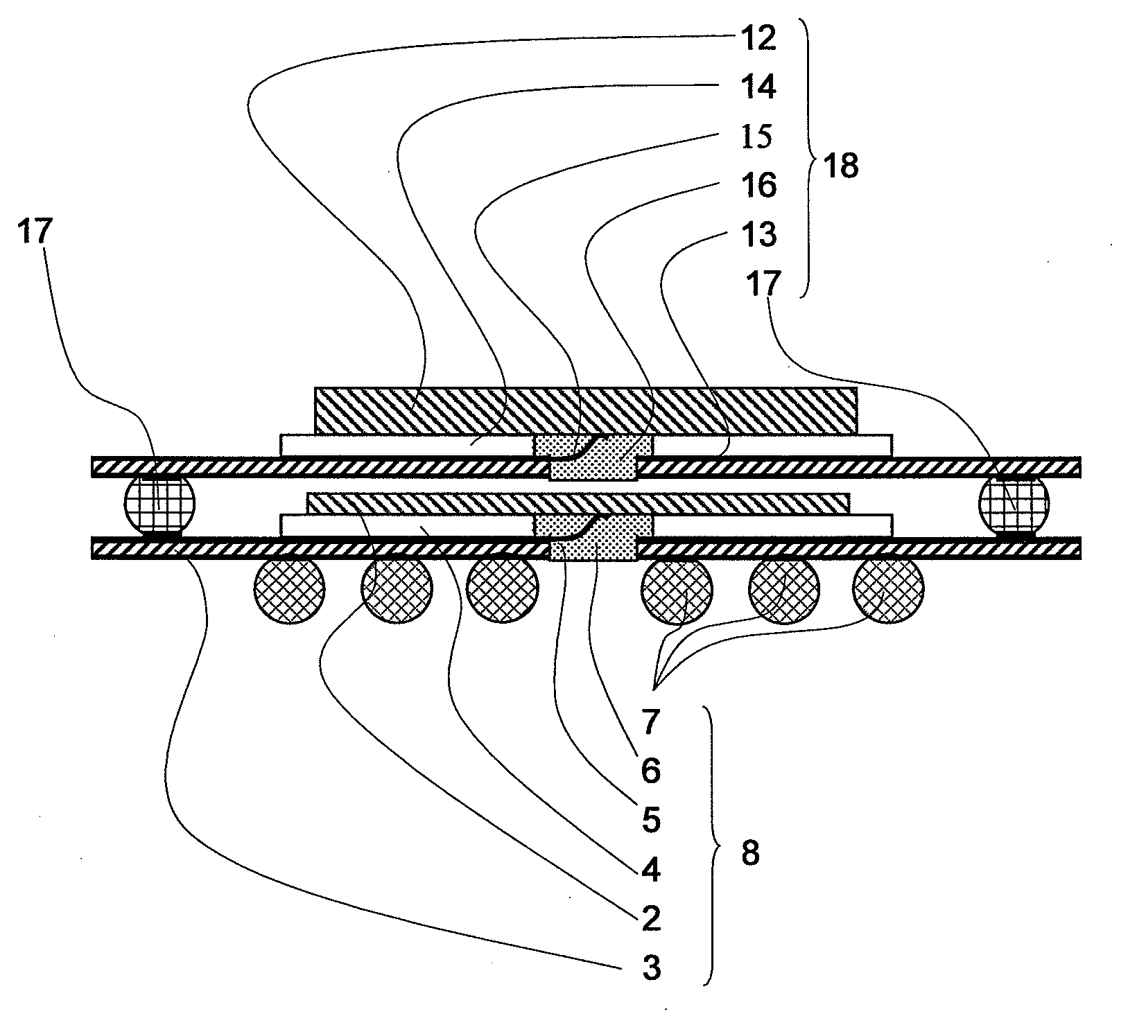
[0031]FIG. 1 is a schematic cross-sectional view of a stacked-type semiconductor device according to a first exemplary embodiment. In the stacked-type semiconductor device in this exemplary embodiment, first FBGA type semiconductor device 8 and second FBGA type semiconductor device 18 are stacked. First semiconductor device 8 comprises first silicon chip 2 that is a first semiconductor chip, tape board 3 that is a wiring board, and solder balls 7 that are external connection terminals.

[0032]Tape board 3 is formed of polyimide with a thickness of about 50 μm. Copper wiring with a thickness of about 20 μm is provided on both surfaces of the polyimide. First silicon chip 2 is mounted on tape board 3 via elastomer 4. Elastomer 4 is a low elastic body with a thickness of about 100 μm.

[0033]Part of the above copper wiring protrudes from tape board 3 and forms lead 5. Lead 5 is connected to a pad (not shown) provided in the center of first silicon chip 2. Thus, first silicon chip 2 and tap...

second exemplary embodiment

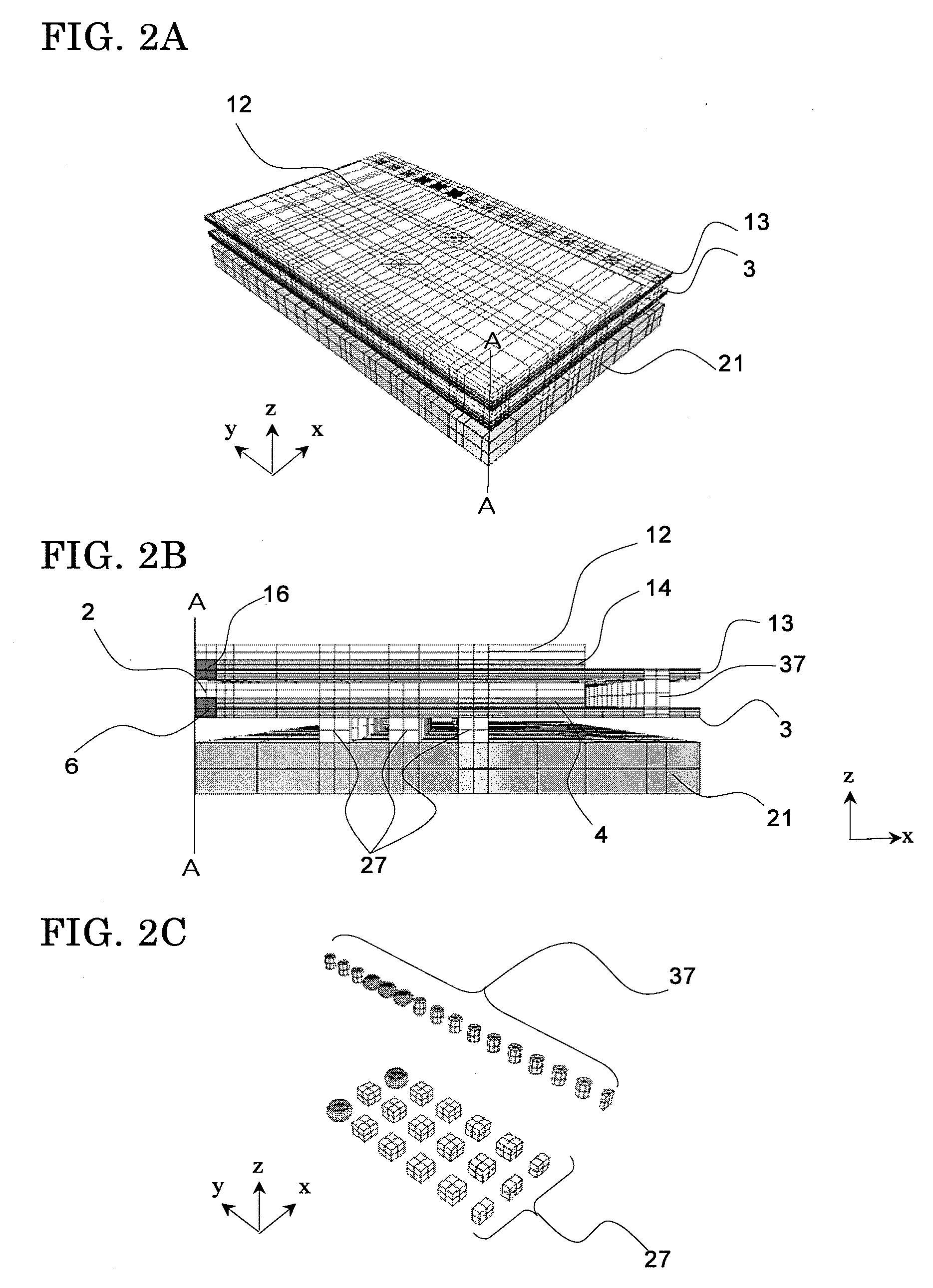
[0052]FIG. 6 is a schematic cross-sectional view of a stacked-type semiconductor device according to a second exemplary embodiment. In the stacked-type semiconductor device according to this exemplary embodiment, a first semiconductor device and three second semiconductor devices are stacked. The configuration of the first and second semiconductor devices is similar to the configuration in the first exemplary embodiment. The first semiconductor device comprises solder balls 7 that are external connection terminals. The three second semiconductor devices comprise solder balls 17 that are inter-board connection terminals.

[0053]The arrangement of solder balls 7 that are external connection terminals conforms to the JEDEC standard. On the other hand, solder balls 17 that are inter-board connection terminals are arranged parallel to each other near both ends of tape board 13 in the second semiconductor device. The thickness of second silicon chip 12 of the second semiconductor device is ...


PUM


Abstract

In a stacked-type semiconductor device, a first semiconductor device and at least one second semiconductor device are stacked. The first semiconductor device includes a wiring board and a first semiconductor chip mounted on the wiring board. The second semiconductor device includes a wiring board and a second semiconductor chip mounted on the wiring board. The thickness of the second semiconductor chip of each second semiconductor device is thicker than the thickness of the first semiconductor chip.

Description

[0001]This application is based upon and claims the benefit of priority from Japanese patent application No. 2008-012816, filed on Jan. 23, 2008, the disclosure of which is incorporated herein in its entirety by reference.BACKGROUND OF THE INVENTION[0002]1. Field of the Invention[0003]The present invention relates to a semiconductor device having a structure in which a plurality of semiconductor devices are stacked.[0004]2. Description of the Related Art:[0005]In recent years, demand for larger memory capacity has further increased. However, due to factors, such as the larger scale, the complexity of peripheral circuits, and the difficulty of shortening of manufacturing process, it is difficult to decrease the area of a semiconductor chip. To achieve larger capacity and higher integration, Japanese Patent Laid-Open No. 2007-165454 describes a chip-stacked-type semiconductor device in which the same or different types of semiconductor chips are stacked.[0006]Also, a stacked-type semi...

Claims


Application Information

Patent Timeline
Patent Type & Authority Applications(United States)
IPC IPC(8): H01L23/02H01L25/10H01L23/48H01L23/485
CPCH01L23/3128H01L2225/1058H01L24/32H01L24/50H01L24/86H01L25/0657H01L25/105H01L2224/29191H01L2225/0652H01L2225/06555H01L2225/06579H01L2924/01005H01L2924/01029H01L2924/0105H01L2924/01082H01L2924/10253H01L2924/15311H01L2924/15331H01L2924/30105H01L2924/3511H01L2924/01006H01L2924/01033H01L2924/014H01L2224/29101H01L24/29H01L2225/1023H01L2924/00
Inventor KATAGIRI, MITSUAKITANIE, HISASHIKAYAMORI, JUNSASAKI, DAIMORIYA, HIROSHI
Owner LONGITUDE LICENSING LTD
Why Eureka
Try Eureka