Heat radiator of semiconductor package

a technology of heat radiator and semiconductor package, which is applied in the direction of semiconductor devices, semiconductor/solid-state device details, lighting and heating apparatus, etc., can solve the problems of insufficient supply of indium, high cost of indium, and damage to the semiconductor elemen

Inactive Publication Date: 2010-07-22
SHINKO ELECTRIC IND CO LTD
View PDF9 Cites 5 Cited by
  • Summary
  • Abstract
  • Description
  • Claims
  • Application Information

AI Technical Summary

Benefits of technology

[0014]Accordingly, embodiments of the present invention may provide a novel and useful heat radiator of a semiconductor package solving one or more of the problems discussed above.

Problems solved by technology

Therefore, unless the temperature of the semiconductor element is forcibly decreased, capacities of the semiconductor element do not work so that the semiconductor element may be damaged.
However, since indium is a rare metal, indium is expensive and a sufficient supply of indium may not be expected in the future.
Therefore, a manufacturing process is complicated.
However, the thermal interface material 300 made by molding the high thermal interface material such as the metal filler or graphite using the resin as a binder has a problem in terms of heat radiation capacities because the thermal conductivity of the resin is not high.
In addition, the carbon nano tubes arranged in the thermally conductive direction have a problem where contact thermal resistance between carbon nano tube end surfaces and the heat radiator is large and therefore expected capacities cannot be achieved.
This is because short carbon nano tubes cannot reach a surface of the heat radiator.
Hence, the thermal conductivity is low and the heat radiation capacities are not good.

Method used


Image

  • Heat radiator of semiconductor package
  • Heat radiator of semiconductor package
  • Heat radiator of semiconductor package

Examples


first embodiment

Heat Radiator of Semiconductor Package of the First Embodiment

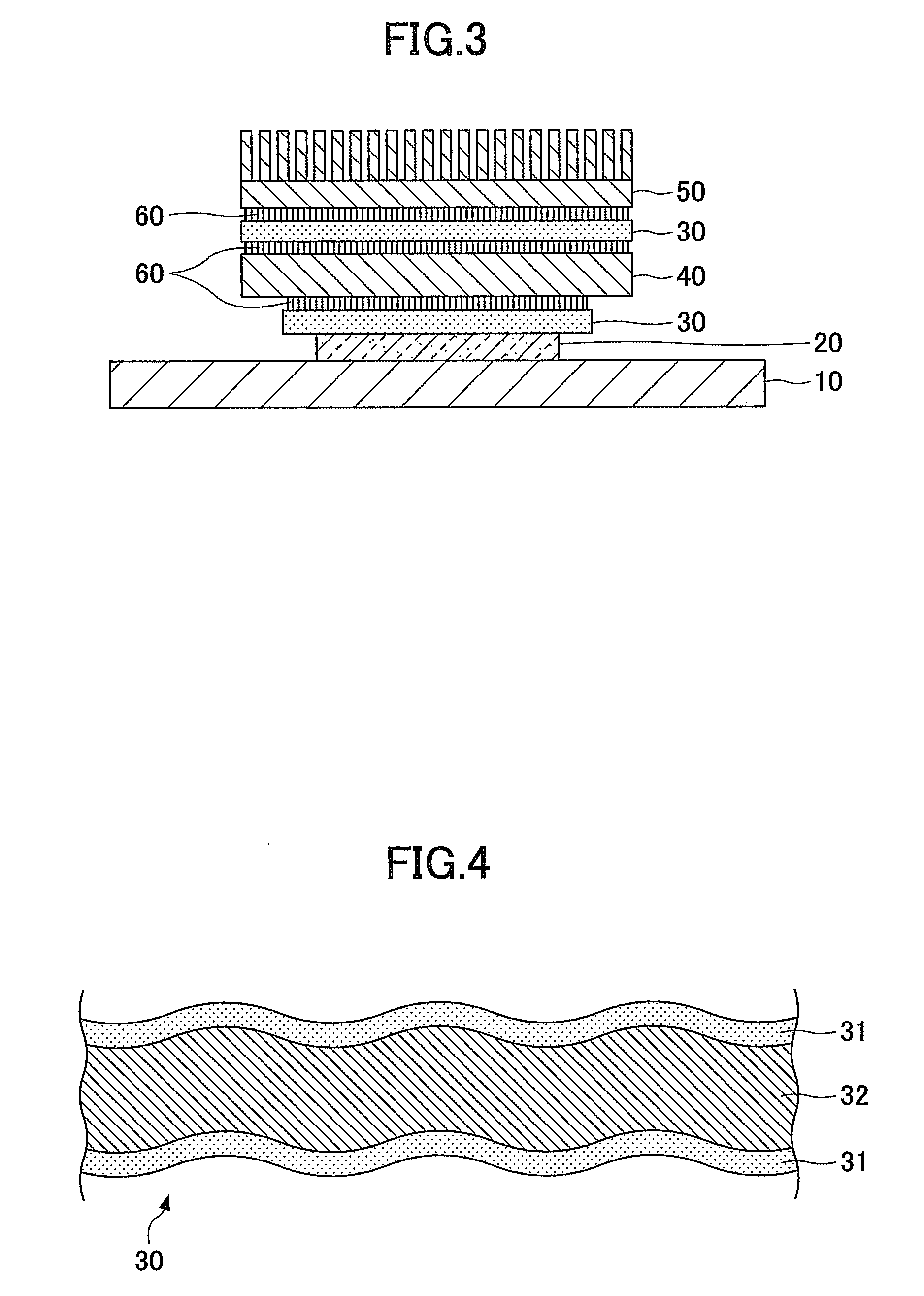
[0034]FIG. 3 is a cross-sectional view showing a heat radiation plate and a heat radiation fin of a first embodiment of the present invention provided on a semiconductor package. As shown in FIG. 3, a heat radiation plate 40 of the first embodiment of the present invention is provided on an upper surface of a TIM 30 as a thermal interface material. The TIM 30 is provided on an upper surface of a semiconductor element 20. The semiconductor element 20 is provided on a board 10. In addition, a heat radiation fin 50 is provided on an upper surface of another TIM 30. This TIM 30 is provided on the upper surface of the heat radiation plate 40.

[0035]The TIM 30 contains a high thermal interface material such as a metal filler, a carbon filler, graphite, or carbon nano tubes. The TIM 30 is molded by using epoxy resin or organic resin as a main ingredient.

[0036]By providing the TIM 30 between the semiconductor element 20 and the he...

modified example 1

of Heat Radiator of Semiconductor Package

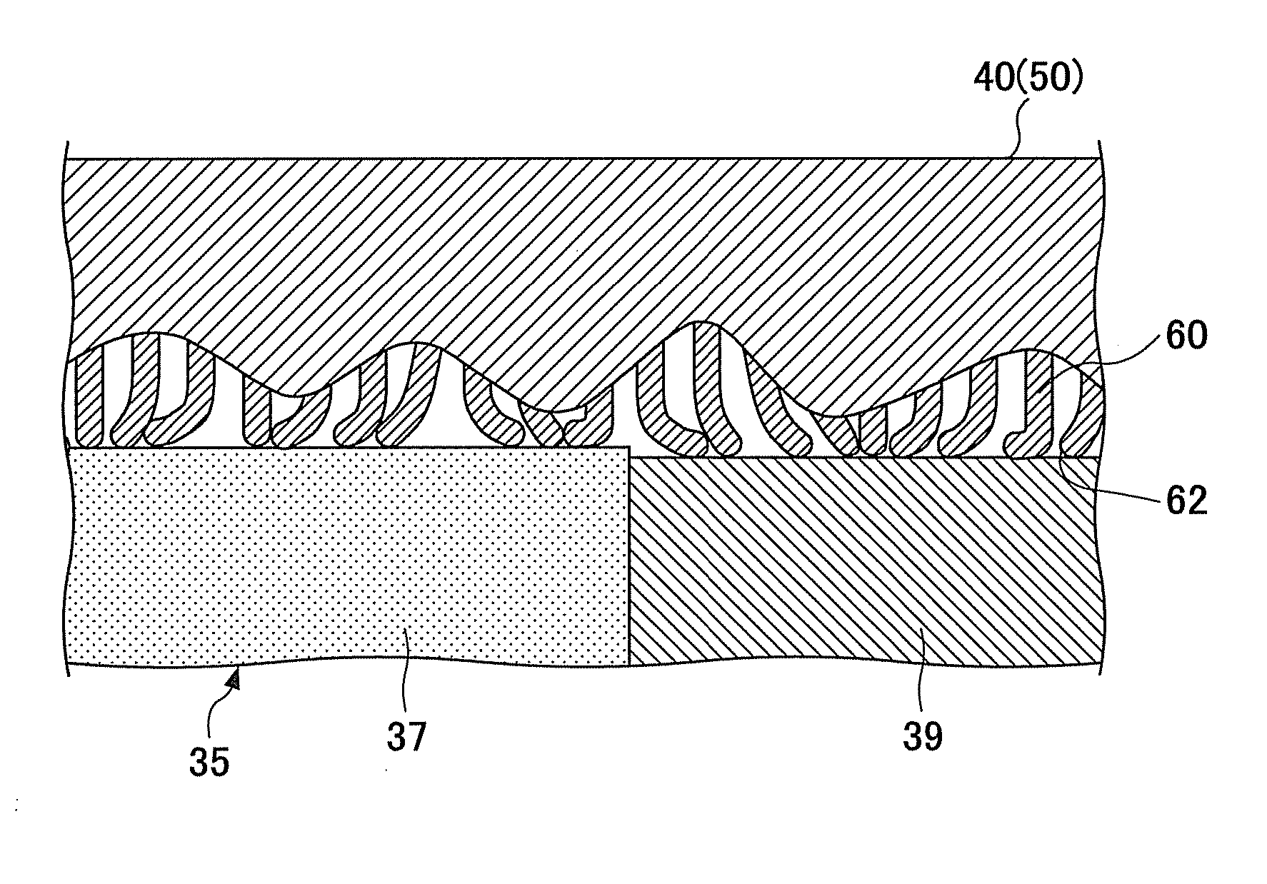
[0064]FIG. 10 is a view showing a TIM where a pillar such as metal or carbon pierces a resin sheet. As shown in FIG. 10, the TIM 35 is a sheet where a pillar such as metal or carbon pierces a resin sheet 37.

[0065]As shown in expanded view in FIG. 10, a position of a horizontal surface of the high thermal interface is slightly lower than a position of resin surface of the resin sheet 37, so that a hollow space is formed. Because of this, if the related art heat radiation plate is used in this case, an air layer is formed at the contact surface of the heat radiation plate and the TIM 35 so that the contact thermal resistance is increased and the thermal conductivity is reduced.

[0066]FIG. 11 is an expanded cross-sectional view of a contact part of the heat radiation plate or the heat radiation fin shown in FIG. 5 and the TIM shown in FIG. 10. As shown in FIG. 11, the carbon nano tubes 60 are formed on the surface of the heat radiation plate 40 o...

second embodiment

Heat Radiator of Semiconductor Package of the Second Embodiment

[0067]In the second embodiment of the present invention, a TIM 70, instead of the TIM 30 of the first embodiment shown in FIG. 3, is used. Other than this, the second embodiment is the same as the first embodiment. Only parts different from the first embodiment are discusses below.

[0068]FIG. 12 is a cross-sectional view of a sheet state TIM molded by resin, the TIM having carbon nano tubes arranged in a thermally conductive direction. As shown in FIG. 12, a TIM 70 has a structure where carbon nano tubes 80 arranged in the thermal conductive direction are molded by resin 80 so that a sheet state is formed. First end parts 82 of the carbon nano tubes 80 project from one surface of the resin 90. Other end parts 84 of the carbon nano tubes 80 project from another surface of the resin 90. The carbon nano tubes 80 correspond to the high thermal interface material 32 of the TIM 30 shown in FIG. 4. The resin 90 is molded by usin...


PUM


Abstract

A heat radiator of a semiconductor package, the heat radiator being provided on the semiconductor package, the heat radiator contacting a thermal interface material, the heat radiator includes a line state high thermal interface material standing, in a thermally conductive direction, on a surface of the heat radiator facing the thermal interface material. Head end parts of the line state high thermal interface material are adhered to a surface of the thermal interface material.

Description

CROSS-REFERENCE TO RELATED APPLICATIONS[0001]This patent application is based upon and claims the benefit of priority of Japanese Patent Application No. 2009-012270 filed on Jan. 22, 2009 the entire contents of which are incorporated herein by reference.BACKGROUND OF THE INVENTION[0002]1. Field of the Invention[0003]The present invention generally relates to heat radiators of semiconductor packages. More specifically, the present invention relates to a heat radiator of a semiconductor package, the heat radiator being provided on the semiconductor package, the heat radiator contacting a thermal interface material.[0004]2. Description of the Related Art[0005]A semiconductor element used for, for example, a CPU (Central Processing Unit) is electrically connected on and fixed to a package. At the time of operation, a temperature of the semiconductor element becomes high. Therefore, unless the temperature of the semiconductor element is forcibly decreased, capacities of the semiconductor...

Claims


Application Information

Patent Timeline
Patent Type & Authority Applications(United States)
IPC IPC(8): H01L23/373F28F21/02
CPCF28F21/02H01L23/373H01L23/3737H01L23/42H01L2924/0002F28F2013/006H01L2924/00
Inventor KOBAYASHI, SUGURU
Owner SHINKO ELECTRIC IND CO LTD
Why Eureka
Try Eureka