On-chip integrated voltage-controlled variable inductor, methods of making and tuning such variable inductors, and design structures integrating such variable inductors

a technology of voltage control and variable inductors, applied in discontinuously variable inductance/transformers, magnets, magnetic bodies, etc., can solve the problems of deteriorating the q value to an unacceptably low value for many mixed signal and radio frequency applications, affecting the overall performance of the related integrated circuit, and limiting components

Inactive Publication Date: 2009-07-30
GLOBALFOUNDRIES INC
View PDF10 Cites 45 Cited by
  • Summary
  • Abstract
  • Description
  • Claims
  • Application Information

AI Technical Summary

Benefits of technology

[0010]In yet another embodiment, a design structure is provided that is embodied in a machine readable medium for designing and manufacturing a circuit. The circuit comprises an on-chip integrated variable inductor including a signal line configured to carry an electrical signal and a ground line positioned proximate to the signal line. The circuit further comprises at least one control unit disposed in a current path connecting the ground line with a ground potential. The at least one control unit is configured to selectively open and close the current path such that the signal line has a first inductance value when the current path is open and a second inductance value when the current path is closed to couple the ground line with the ground potential. The circuit and circuit structure reside in design files or design structures (e.g. GDSII files), which can be transferred to design houses, manufacturers, customers, or another third party.

Problems solved by technology

The performance of an inductor significantly affects the overall performance of the related integrated circuit and may even be a performance limiting component.
However, conventional arrangements require some type of switch in the signal line of the variable inductor, which may deteriorate the Q value to an unacceptably low value for many mixed signal and radio frequency applications.

Method used


Image

  • On-chip integrated voltage-controlled variable inductor, methods of making and tuning such variable inductors, and design structures integrating such variable inductors
  • On-chip integrated voltage-controlled variable inductor, methods of making and tuning such variable inductors, and design structures integrating such variable inductors
  • On-chip integrated voltage-controlled variable inductor, methods of making and tuning such variable inductors, and design structures integrating such variable inductors

Examples


Embodiment Construction

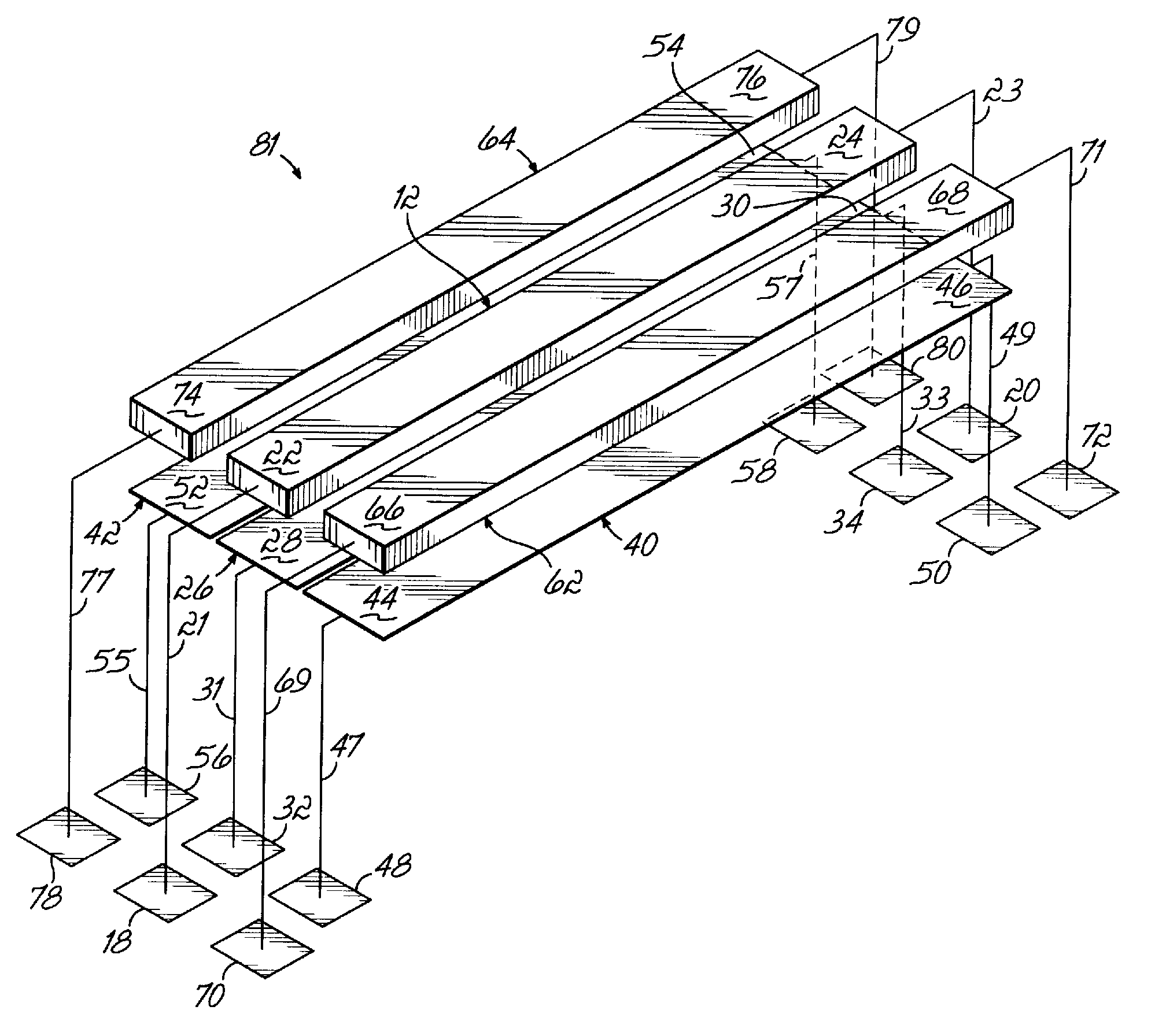
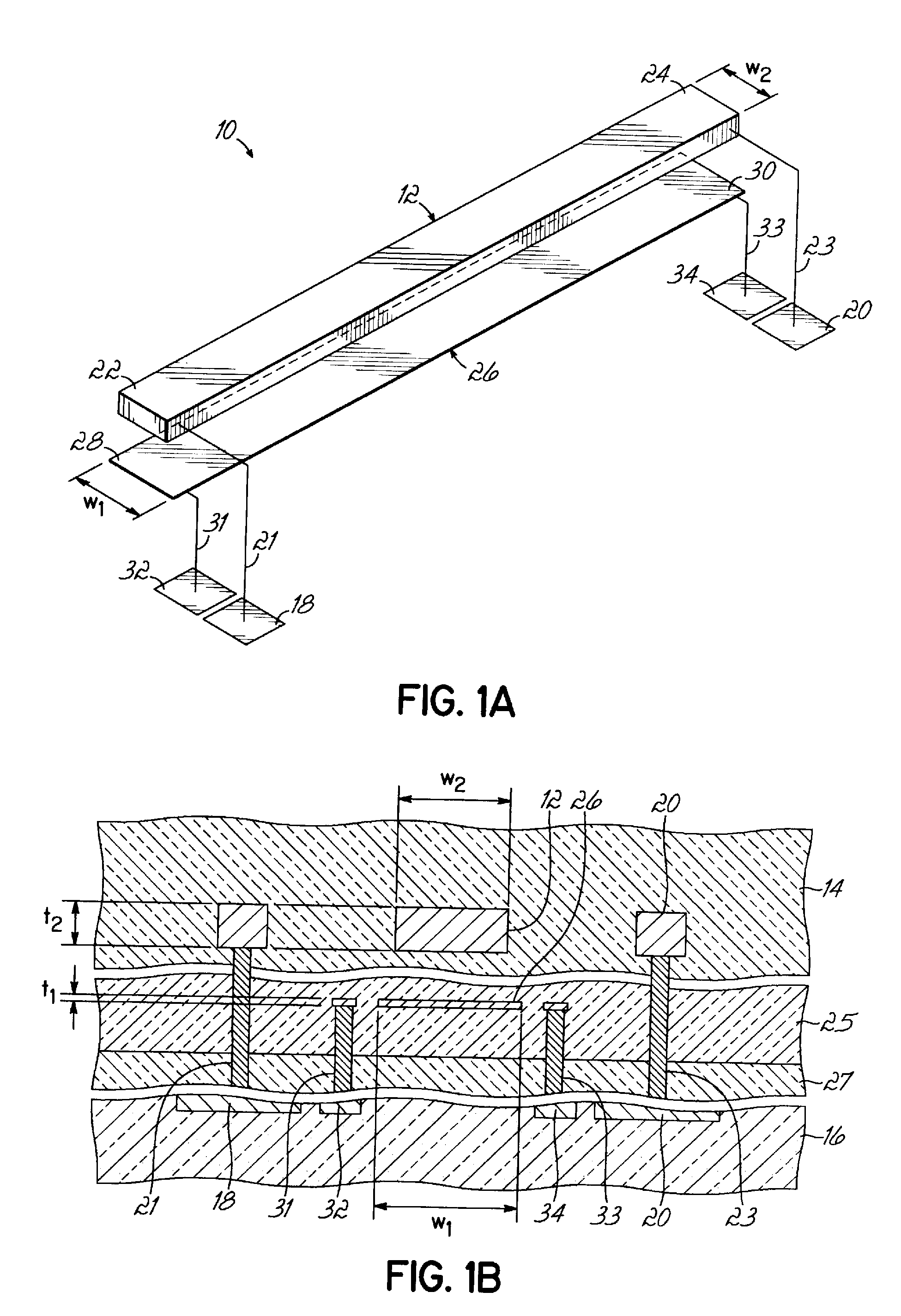
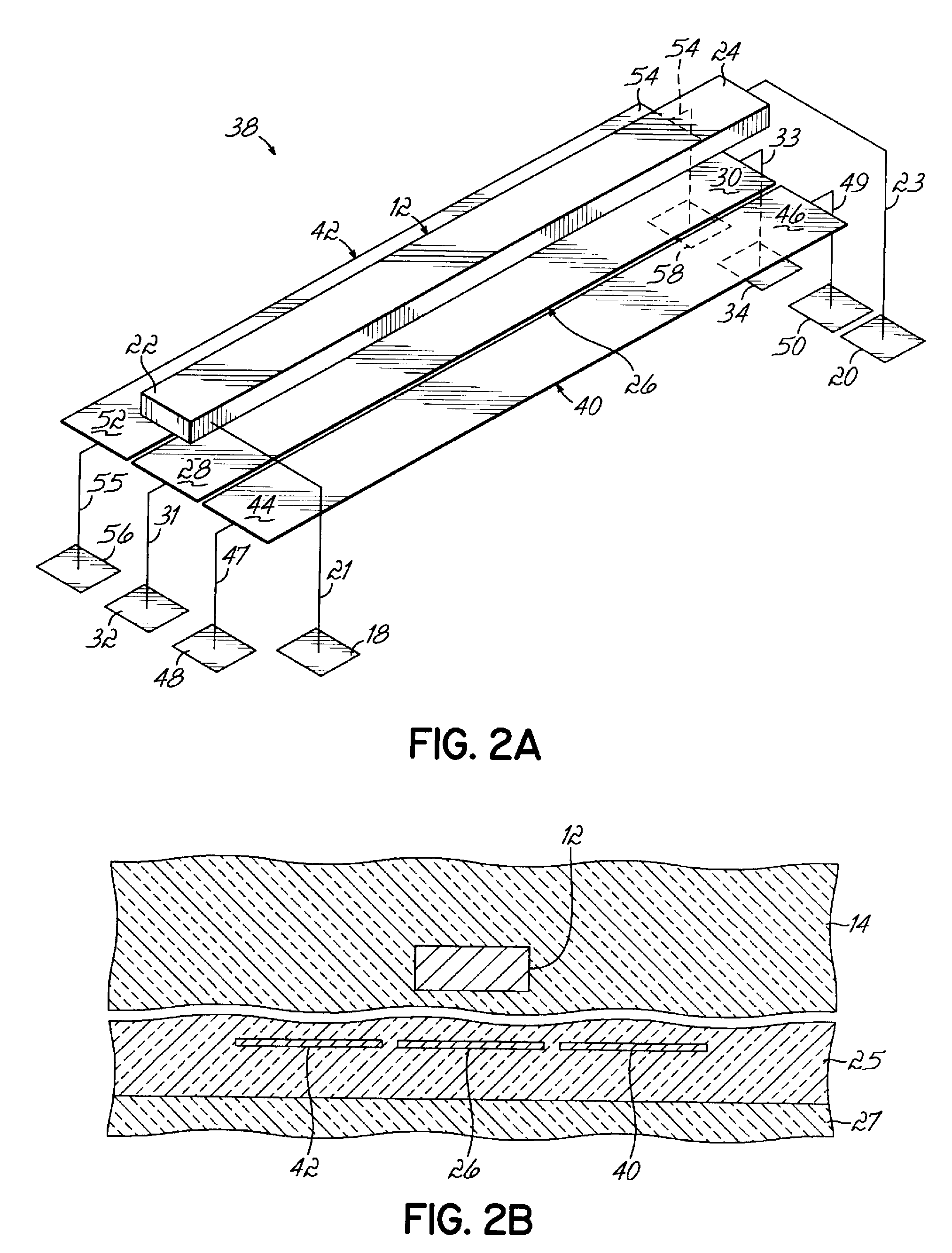
[0023]With reference to FIGS. 1A and 1B, an on-chip integrated variable inductor, which is generally indicated by reference numeral 10, consists of a signal line 12 in the representative form of a strip of a conductive material that is buried in, and surrounded by, an insulating layer 14 (FIG. 1B) of a dielectric material. The inductor 10 is carried on a substrate 16, which includes at least one integrated circuit formed thereon and / or therein with devices having features, of which features 18, 20 are representative, that are contacted with the signal line 12. The features 18, 20 may comprise metallization lines, a contact, a semiconductor material, and / or features of circuit elements previously formed on and / or in the substrate 16. The substrate 16 is typically a chip or die comprising a piece of a semiconductor wafer containing an entire integrated circuit.

[0024]Ports or terminals 22, 24 located at opposite ends of the signal line 12 are electrically coupled by conductive paths 21...


PUM

PropertyMeasurementUnit
aspect ratioaaaaaaaaaa
dielectric constantaaaaaaaaaa

Abstract

On-chip integrated variable inductors, methods of making and tuning an on-chip integrated variable inductor, and design structures embodying a circuit containing the on-chip integrated variable inductor. The inductor generally includes a signal line configured to carry an electrical signal, a ground line positioned in proximity to the signal line, and at least one control unit electrically coupled with the ground line. The at least one control unit is configured to open and close switch a current path connecting the ground line with a ground potential so as to change an inductance of the signal line.

Description

FIELD OF THE INVENTION[0001]The invention relates generally to integrated circuits and, in particular, to on-chip integrated variable inductors for integrated circuits, design structures embodying the on-chip integrated variable inductors, methods for fabricating on-chip integrated variable inductors, and methods for tuning an on-chip integrated variable inductor during circuit operation.BACKGROUND OF THE INVENTION[0002]Inductors are passive electrical devices found in many integrated circuits, including radiofrequency integrated circuits (RFICs), multiple band passive matching networks, multiple band voltage control oscillator (VCO) tank circuits, and phase delay units. Inductors may be used singularly in an integrated circuit or arranged in pairs as differential inductors or transformers in the integrated circuit. In general, an inductor is a reactive element that can store energy in its magnetic field and tends to resist a change in the amount of current flowing through it. The p...

Claims


Application Information

Patent Timeline
Patent Type & Authority Applications(United States)
IPC IPC(8): H01F21/00H01F41/04H01F5/00
CPCH01F17/0006Y10T29/4902H01F21/12H01F21/005
Inventor DING, HANYIMINA, ESSAM F.WOODS, WAYNE H.
Owner GLOBALFOUNDRIES INC
Why Eureka
Try Eureka