

Sensing Structure
- Summary
- Abstract
- Description
- Claims
- Application Information
AI Technical Summary
Benefits of technology
Problems solved by technology
Method used
Image

Examples
second embodiment
[0028]FIG. 4 depicts the sensing structure of this invention. In this embodiment, the sensing chip may be omitted and the driving chip 31 may be retained. In this case, through the first connecting portion 25 and the third connecting portion 27 of the FPC 24, the sensing signal from the sensing unit 23 is transmitted to the signal processing system (not shown) for processing information. Moreover, the sensing chip and the driving chip may be integrated in the embodiment. The driving chip 31 with a sensing function may be used. In other words, through the first connecting portion 25 and the second connecting portion 26, the sensing signal generated by the sensing unit 23 may be transmitted to the driving chip 31 for processing information. And then the signal from the driving chip 31 is transmitted to the signal processing system (not shown) through the second connecting portion 26 and the third connecting portion 27. In this embodiment, a chip with driving and sensing functions is u...
third embodiment
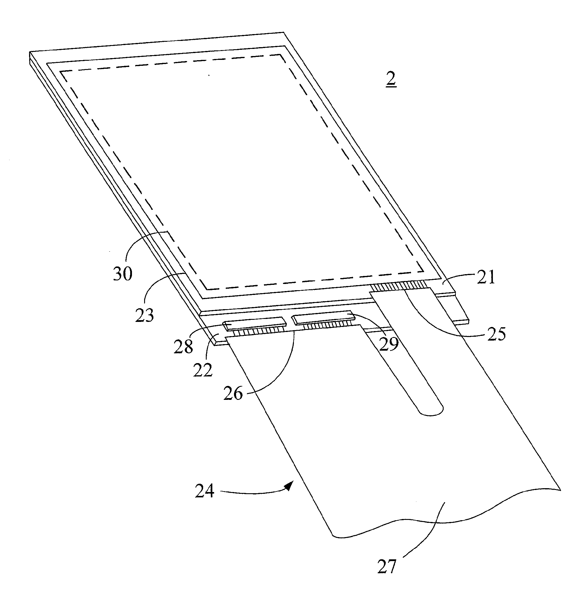
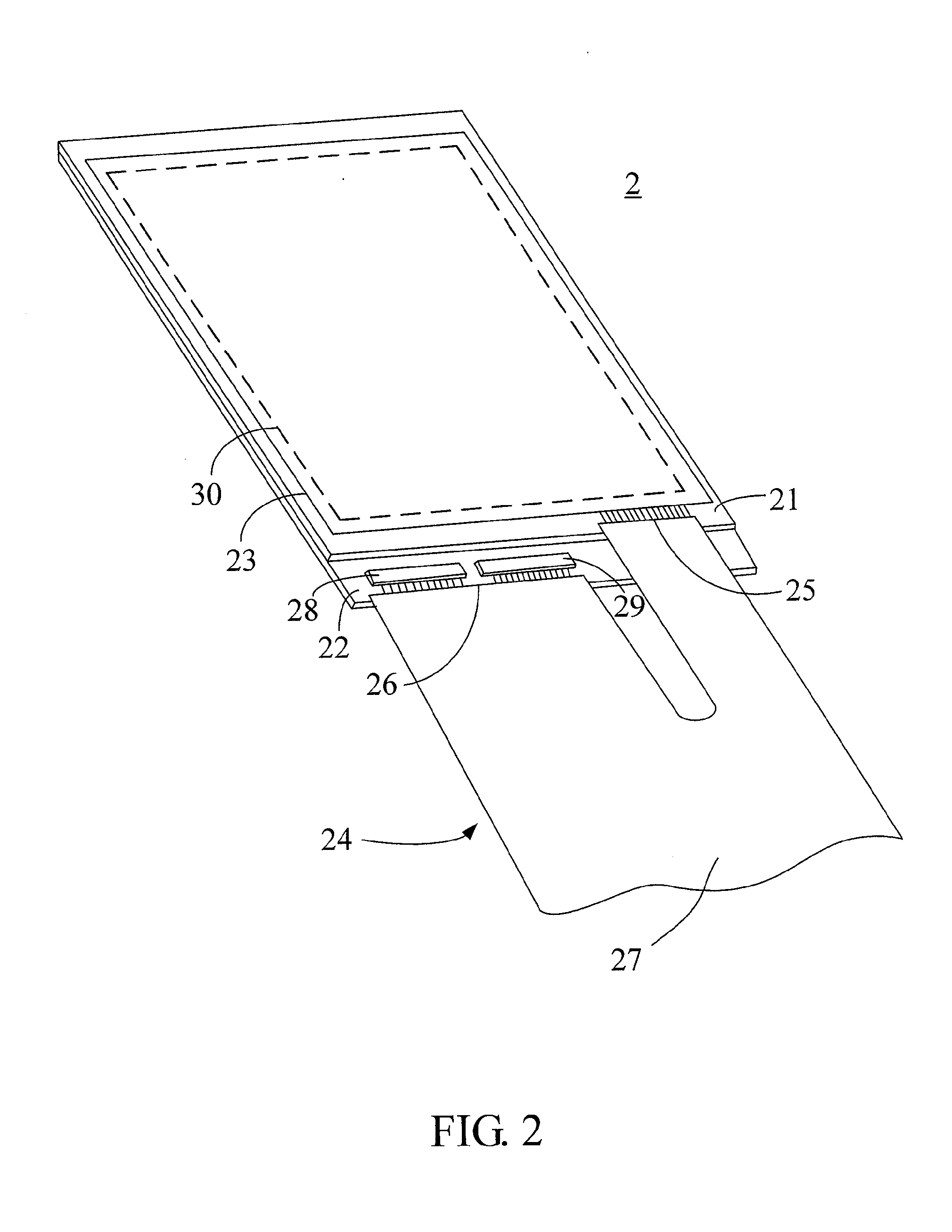
[0029]FIG. 5 depicts the sensing structure of this invention. In this embodiment, the sensing unit 23, the sensing chip 28 and the driving chip 29 electrically connect to the FPC 24 respectively, and a first connecting portion 25 is between two separate second connecting portions 26. In more detail, at the first end, the FPC 24 has one first connecting portion 25 electrically connecting to the sensing unit 23 and two separate second connecting portions 26 connecting to the second substrate 22. As depicted in FIG. 5, the two separate second connecting portions 26 are disposed corresponding to the sensing chip 28 and the driving chip 29 respectively. The two separate second connecting portions 26 connect with different locations of the second substrate 22 respectively, and the first connecting portion 25 is located between the two separate second connecting portions 26. Similarly, for the facileness of heat bonding and for the precision of circuit alignment, slits may be formed betwee...
fourth embodiment
[0030]FIG. 6 depicts the sensing structure of this invention. In this embodiment, the sensing chip 28 and the driving chip 29 may be separately disposed on different locations of the second substrate 22. The FPC 24 electrically connects to the sensing unit 23, the sensing chip 28, and the signal processing system (not shown). The driving chip 29 electrically connects with another FPC 32 for independently transmitting the driving signal from the signal processing system. The location of the first connecting portion 25 may be changed. For example, the sensing chip 28 and the driving chip 29 are disposed adjacent to each other, and the first connecting portion 25 is disposed on the different location of the first substrate 21. However, the above description is for illustration, and those skilled in the art may make an adjustment depending on the practical requirements. Likewise, the dimensions, locations and numbers of chips are not limited. Those skilled in the art may make an adjustm...
PUM
 Abstract
Description
Claims
Application Information