Organic light emitting diode display device and method of fabricating the same

a technology of light-emitting diodes and display devices, which is applied in the direction of coatings, electroluminescent light sources, electric lighting sources, etc., can solve the problems of additional material costs of spacer films

Active Publication Date: 2009-08-06
SAMSUNG DISPLAY CO LTD
View PDF6 Cites 26 Cited by
  • Summary
  • Abstract
  • Description
  • Claims
  • Application Information

AI Technical Summary

Benefits of technology

[0018]Aspects of embodiments of the present invention are directed toward an organic light emitting diode (OLED) display device and a method of fabricating the same, in which when an organic layer having an emission layer (EML) is formed using a deposition mask, damage to a pixel defining layer due to the unevenness of the deposition mask is prevented or reduced using spherical spacers disposed on the pixel defining layer, so that a conventional photolithography process for forming a spacer pattern is omitted.

Problems solved by technology

However, in this conventional method of fabricating the OLED display device, an extra photolithography process for forming the spacer pattern is added, and additional material costs for the spacer film are incurred.

Method used


Image

  • Organic light emitting diode display device and method of fabricating the same
  • Organic light emitting diode display device and method of fabricating the same
  • Organic light emitting diode display device and method of fabricating the same

Examples


Embodiment Construction

[0035]In the following detailed description, only certain exemplary embodiments of the present invention are shown and described, by way of illustration. As those skilled in the art would recognize, the invention may be embodied in many different forms and should not be construed as being limited to the embodiments set forth herein. Furthermore, in the context of the present application, when an element is referred to as being “on” another element, it can be directly on the another element or be indirectly on the another element with one or more intervening elements interposed therebetween. Like reference numerals designate like elements throughout the specification.

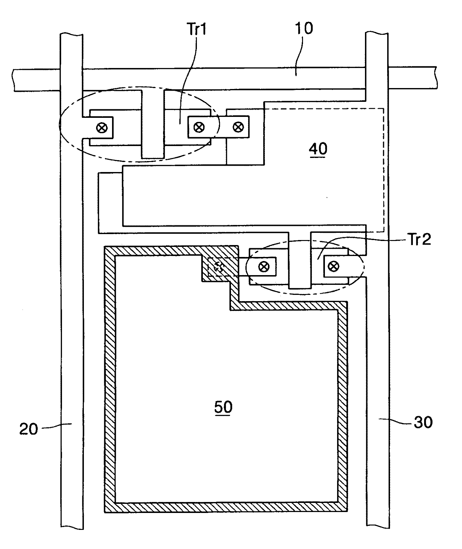
[0036]FIG. 3 is a plan schematic view of a unit pixel of a general organic light emitting diode (OLED) display device.

[0037]Referring to FIG. 3, the unit pixel includes a switching transistor Tr1, a driving transistor Tr2, a capacitor 40, and an OLED 50. A gate line 10, a data line 20, and a power supply line 30 are conn...


PUM


Abstract

An organic light emitting diode (OLED) display device and a method of fabricating the same are provided. When an organic layer having an emission layer (EML) is formed using a deposition mask, damage to a pixel defining layer due to inconsistencies or unevenness of the deposition mask is prevented or reduced using spherical spacers disposed on the pixel defining layer. A plurality of spherical spacers are applied on the pixel defining layer prior to forming an opening in the pixel defining layer exposing the first electrode. An organic layer having an emission layer (EML) is formed on the first electrode at the opening by using a deposition mask. The spherical spacers prevent or reduce damage to the pixel defining layer caused by inconsistencies or unevenness in the deposition mask by maintaining a spacing between the pixel defining layer and the deposition mask.

Description

CROSS-REFERENCE TO RELATED APPLICATION[0001]This application claims the priority of and the benefit of Korean Patent Application No. 2008-10244, filed Jan. 31, 2008, the disclosure of which is hereby incorporated herein by reference in its entirety.BACKGROUND OF THE INVENTION[0002]1. Field of the Invention[0003]The present invention relates to an organic light emitting diode (OLED) display device and a method of fabricating the same.[0004]2. Description of the Related Art[0005]In general, an organic light emitting diode (OLED) includes an organic layer interposed between a first electrode (i.e., an anode) and a second electrode (i.e., a cathode). The first electrode is a transparent electrode formed of, for example, indium tin oxide (ITO), and the second electrode is formed of a metal having a low work function, such as Ca, Li, or Al. When a forward voltage is applied to the OLED, holes emitted from the anode combine with electrons emitted from the cathode to form excitons, and whil...

Claims


Application Information

Patent Timeline
Patent Type & Authority Applications(United States)
IPC IPC(8): H01L51/52B05D5/06H05B44/00
CPCH01L51/0011H01L27/3246H10K59/122H10K71/166H05B33/22H05B33/10H10K71/00
Inventor KWON, JUNG-HYUN
Owner SAMSUNG DISPLAY CO LTD
Why Eureka
Try Eureka