Active matrix substrate and liquid crystal display device provided with same

a technology of active matrix substrate and liquid crystal display device, which is applied in the direction of semiconductor devices, instruments, optics, etc., can solve the problems of reducing efficiency percentage, needing etching for a remarkably long period of time, and reducing mobility, so as to reduce signal delay and reduce signal delay

Inactive Publication Date: 2009-08-13
SHARP KK
View PDF20 Cites 61 Cited by
  • Summary
  • Abstract
  • Description
  • Claims
  • Application Information

AI Technical Summary

Benefits of technology

[0017]In view of the problems described above, preferred embodiments of the present invention provide an active matrix substrate and a liquid crystal display device including the same that has both a decreased signal delay caused by resistance and a decreased signal delay caused by parasitic capacitance.

Problems solved by technology

As a result, a problem of a decrease in mobility occurs.
Therefore, polysiliconization of the transparent electrodes causes a need to etch for a remarkably long period of time.
This causes a problem that an efficiency percentage decreases, such as occurrence of leaking from the metal thin film formed on the upper layer.
Consequently, the common electrodes formed at the CS wires 123 have a high resistance, which causes a problem of signal delay.
However, in order to solve this problem, if a width of the CS wires 123 is thickened so as to aim for a low resistance, another problem occurs that an aperture ratio decreases.
Therefore, defects such as a shortage and the like may possibly occur, and a parasitic capacitance between the gate and source bus lines and the CS wires increases.

Method used


Image

  • Active matrix substrate and liquid crystal display device provided with same
  • Active matrix substrate and liquid crystal display device provided with same
  • Active matrix substrate and liquid crystal display device provided with same

Examples


first preferred embodiment

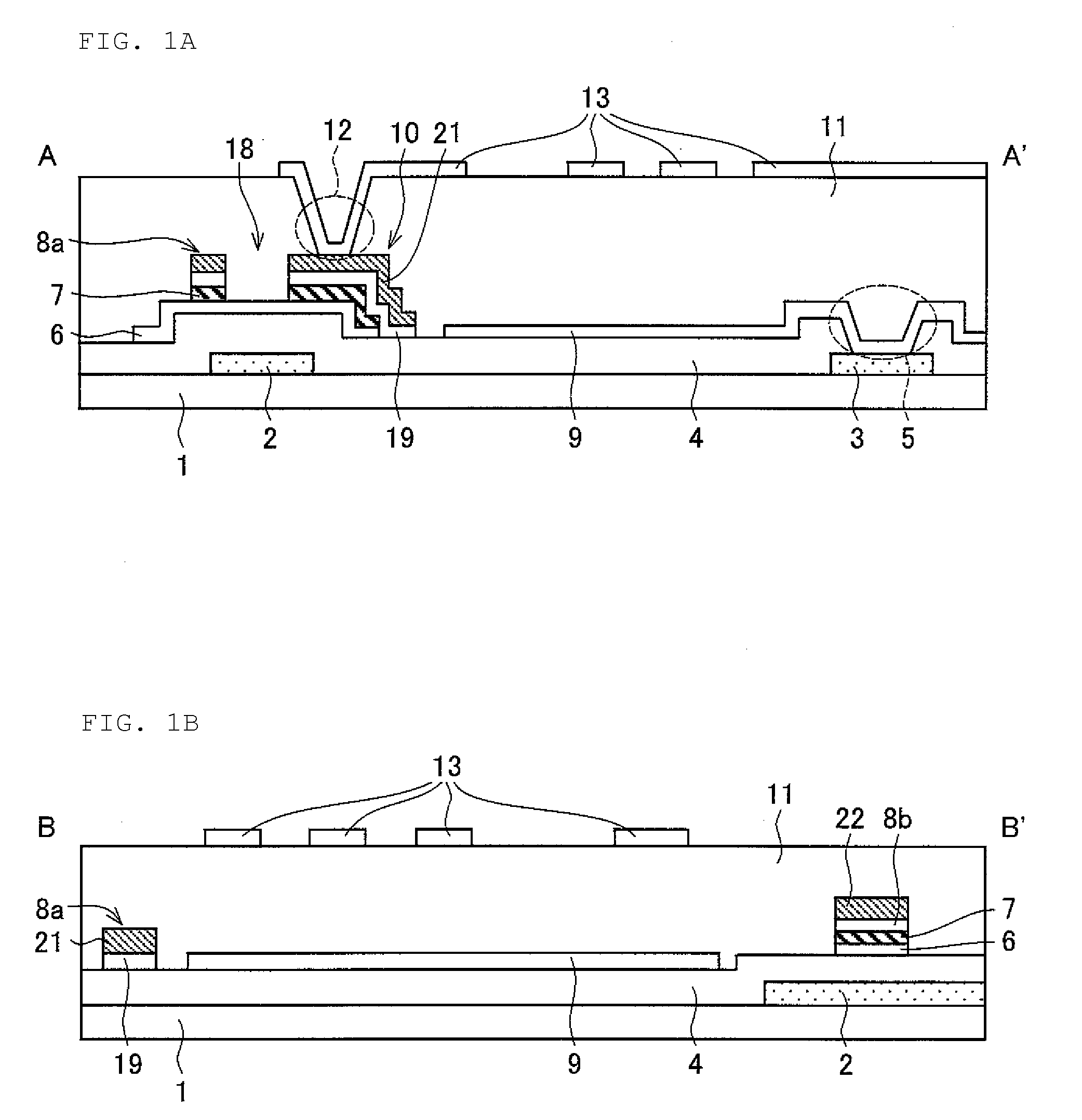
[0111]FIGS. 4A and 4B illustrate a first preferred embodiment, wherein FIG. 4A is a cross sectional view taken along a line A-A′ corresponding to FIG. 1A, and FIG. 4B is a cross sectional view taken along a line B-B′ corresponding to FIG. 1B. A plane view of the first preferred embodiment is identical to FIG. 2. Therefore, the plane view of the first preferred embodiment is omitted here.

[0112]The preferred embodiment has a single-layered interlayer insulating film 11 as illustrated in FIGS. 1A and 1B. In comparison, the first preferred embodiment has a double-layered interlayer insulating film 11, as illustrated in FIGS. 4A and 4B. More specifically, in the first preferred embodiment, the interlayer insulating film 11 is so arranged as a double-layered structure including an inorganic film 23 made of SiNx, SiO2 or the like, and a film 24 made of low-dielectric constant organic material.

[0113]This allows for reduction of parasitic capacitance as compared to the preferred embodiment. ...

second preferred embodiment

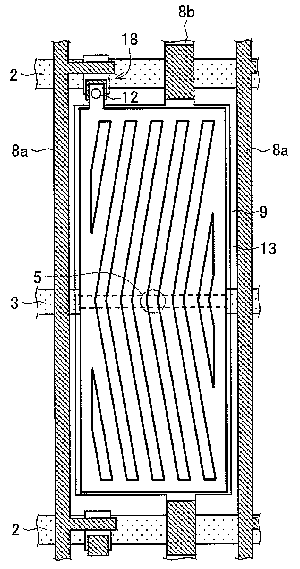
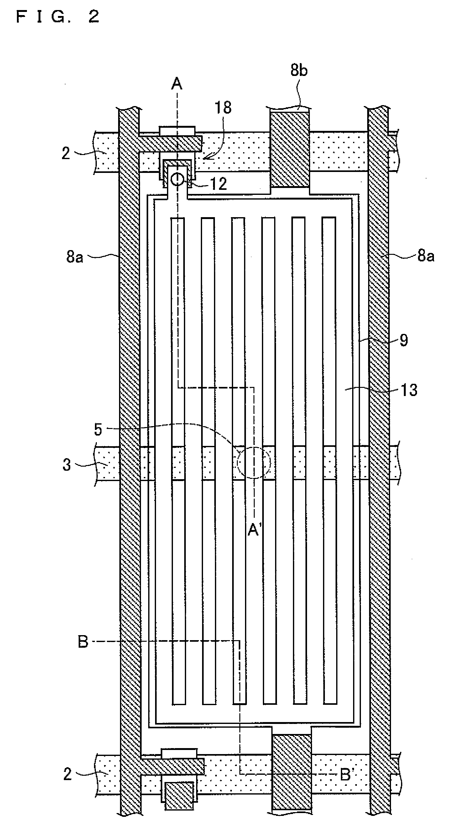
[0118]FIG. 5 illustrates a second preferred embodiment, and is a plane view corresponding to FIG. 2. In addition, FIG. 6A is a cross sectional view taken along a line A-A′ as indicated in FIG. 5, and FIG. 6B is a cross sectional view taken along a line B-B′ as indicated in FIG. 5.

[0119]In the preferred embodiment shown in FIG. 2, the auxiliary common electrode wires 3 are arranged substantially at a midpoint between adjacent gate wires 2, respectively. In comparison, the second preferred embodiment arranges the auxiliary common electrode wires 3 in a vicinity of one of the respective adjacent gate wires 2. More specifically, the auxiliary common electrode wires 3 has a section that does not overlap with the pixel electrodes 13 in an extending direction of the source wires 8a. That is to say, the auxiliary common electrode wires 3 juts out from the pixel electrodes 13 in the extending direction of the source wires 8a. Moreover, the second preferred embodiment has a contact hole 5′ at...

third preferred embodiment

[0130]FIG. 7 illustrates a third preferred embodiment, and is a plane view corresponding to FIG. 2. In addition, FIG. 8A is a cross sectional view taken along a line A-A′ as indicated in FIG. 7, FIG. 8B is a cross sectional view taken along a line B-B′ as indicated in FIG. 7.

[0131]The third preferred embodiment, in addition to the arrangement of the preferred embodiment shown in FIG. 2, has the auxiliary common electrode wires 3 extend to an outer peripheral section (disabled area) of the pixel area, and extend in the outer peripheral section so as to be parallel or substantially parallel to the source wires 8a, as illustrated in FIG. 7. In other words, the auxiliary common electrode wires 3 are extended to a surrounding section (outer peripheral section) of the common electrodes 9, and extended in the surrounding section so as to be parallel or substantially parallel to the source wires 8a. Namely, as illustrated in FIG. 7, a shape of the auxiliary common electrode wires 3 from a p...


PUM

PropertyMeasurementUnit
temperatureaaaaaaaaaa
dielectric constantaaaaaaaaaa
thicknessaaaaaaaaaa

Abstract

An active matrix substrate includes an insulating substrate, gate wires and source wires that intersect with each other on the insulating substrate, and TFTs provided at intersections of signal lines. The TFTs include gate electrodes, source electrodes and drain electrodes, respectively. A transparent conductive film, which is arranged to be used as a lower layer of the sources and the drains, is used as common electrodes for pixel areas surrounded by adjacent source wires, and also common electrode wires arranged to connect adjacent ones of the common electrodes parallel or substantially parallel to the source wires. This provides an active matrix substrate in which a signal delay caused by resistance and parasitic capacitance is reduced.

Description

BACKGROUND OF THE INVENTION[0001]1. Field of the Invention[0002]The present invention relates to an active matrix substrate which incorporates a TFT, and a liquid crystal display device including the active matrix substrate.[0003]2. Description of the Related Art[0004]Liquid crystal display devices of an FFS (Fringe Field Switching) mode have been known in the art. A liquid crystal display device of the FFS mode is arranged such that a counter electrode and a pixel electrode (i) are formed by transparent material such as ITO, (ii) have a narrower space between the counter electrode and the pixel electrode than a space between the upper and lower substrates, and (iii) have a width between the counter electrode and the pixel electrode in a degree in which all of liquid molecules aligned on an upper part of an electrode are drivable.[0005]The liquid crystal display device of the FFS mode can attain a higher aperture ratio than that of a liquid crystal display device of an IPS (In-Place...

Claims


Application Information

Patent Timeline
Patent Type & Authority Applications(United States)
IPC IPC(8): G02F1/1343
CPCG02F1/134363G02F1/136227G02F1/1368G02F2001/13606H01L27/1248G02F2001/13629G02F2201/121H01L27/124G02F2001/136263G02F1/13606G02F1/136263G02F1/13629H01L27/1214
Inventor MURAI, ATSUHITO
Owner SHARP KK
Why Eureka
Try Eureka