Method for fabricating pixel array substrate

a technology of pixel array and substrate, applied in non-linear optics, instruments, optics, etc., can solve the problems of reducing the display quality of the pixel array substrate, the cost of making optical masks the delay is even more serious, so as to reduce the cost of fabricating and reduce the delay of data signals

Active Publication Date: 2009-10-06
AU OPTRONICS CORP
View PDF12 Cites 27 Cited by
  • Summary
  • Abstract
  • Description
  • Claims
  • Application Information

AI Technical Summary

Benefits of technology

[0010]An objective of the present invention is to provide a pixel array substrate and method for fabricating the same, by which the production cost for fabricating the same can be reduced and the problem of data signal delay can be avoided.
[0019]In summary, in accordance with the pixel array substrate and the method for fabricating the same of the present invention, both the data line patterns and the scan lines are derived from the first conductive layer, thus they are made of the same kind material. The data lines are substantially composed of the data line patterns. Therefore, the data lines and the scan lines have approximate sheet resistance, by which the data signal delay can be reduced. Furthermore, comparing with the conventional technology that requires five optical masks, the present invention only employs three optical masks for fabricating the pixel array substrate. Accordingly, the fabricating cost can be reduced.

Problems solved by technology

As such, a delay of data signal transmit will occur, which decreases display quality of the pixel array substrate 100.
Particularly, larger pixel array substrates are become more popular; if the pixel array substrate has a larger size, the delay would be even more serious.
The cost for making optical masks is one of the considerable expenses for fabricating such a pixel array substrate 100.
Unfortunately, according to the above-illustrated process, five different optical masks are required for fabricating such a pixel array substrate 100.
Therefore, it is hard to reduce production cost addressing to such a process.
Particularly, when a larger pixel array substrate 100 is to be fabricated, larger optical masks are correspondingly required, thus the production cost has to be further increased.

Method used


Image

  • Method for fabricating pixel array substrate
  • Method for fabricating pixel array substrate
  • Method for fabricating pixel array substrate

Examples


Embodiment Construction

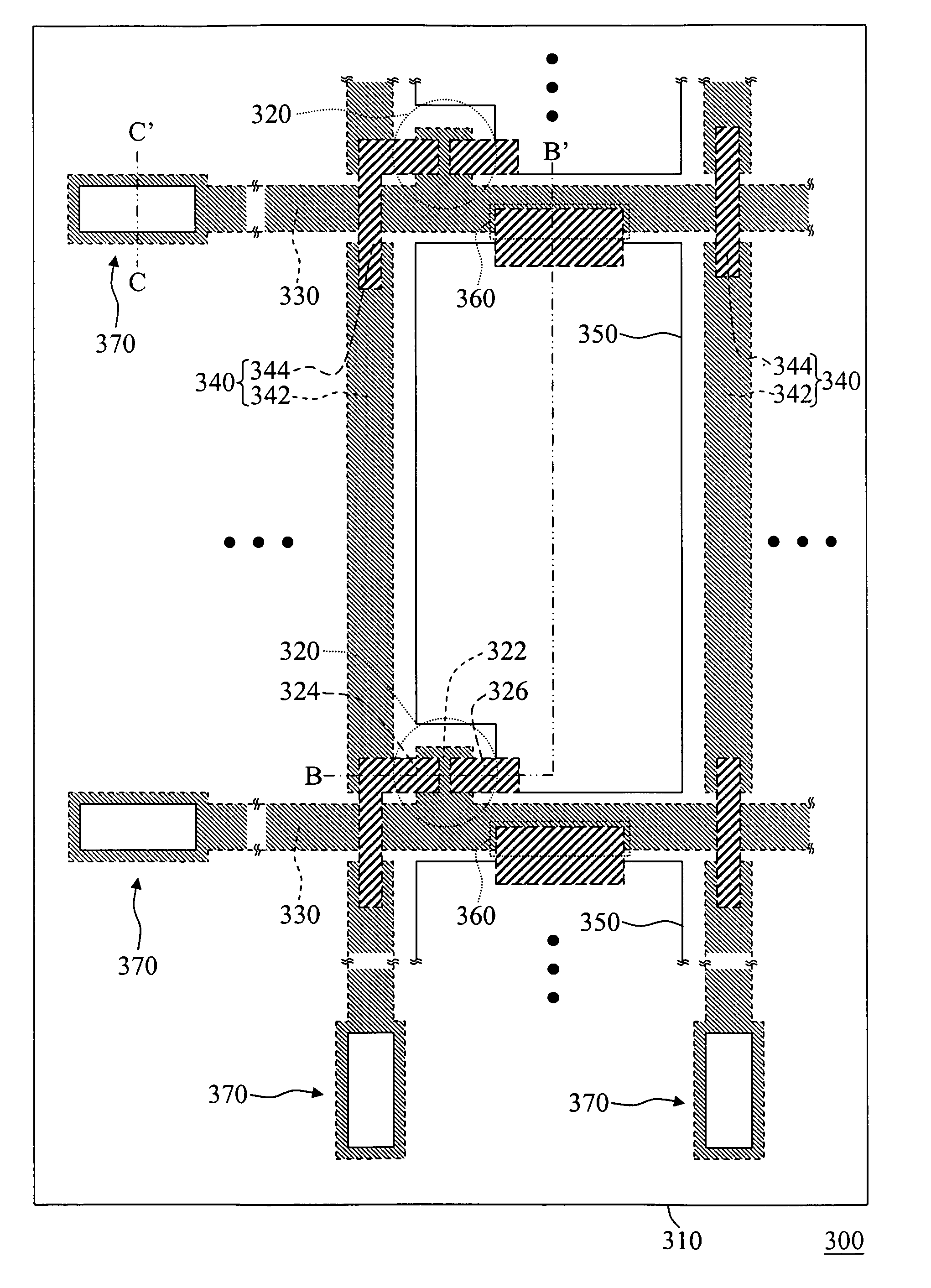
[0028]FIG. 3 is a partial top view of a pixel array substrate according to an embodiment of the present invention, while FIGS. 4A to 4F are respective cross-sectional views along lines B-B′ and C-C′ shown in FIG. 3 for illustrating a step flow for fabricating a pixel array substrate of FIG. 3. As shown in FIG. 3, a pixel array substrate 300 according to the present invention includes a substrate 310, a plurality of active devices 320, a plurality of scan lines 330, a plurality of data lines 340, and a plurality of pixel electrodes 350. The active devices 320 are disposed on the substrate 310 and each of the active devices 320 is electrically connected with a corresponding scan line 330, a corresponding data line 340 and a corresponding pixel electrode 350. Each of the data line 340 includes a plurality of data line patterns and a plurality of contacting portions 344. The contacting portions 344 are electrically connected with the data lines 342, and each of the contacting portions 3...


PUM

PropertyMeasurementUnit
transparentaaaaaaaaaa
conductiveaaaaaaaaaa
thicknessaaaaaaaaaa

Abstract

A method for fabricating a pixel array substrate is provided. The method includes: forming a plurality of gate electrodes, a plurality of scan lines, a plurality of data line patterns and a plurality of pixel electrode patterns on a substrate; then forming a channel over each of the gate electrodes and a plurality of contact window openings for exposing the data line patterns; then forming a plurality of contact windows electrically connected with the data line patterns; and then forming a plurality of contacting portions which are electrically connected with the contact windows, a plurality of source electrodes which are electrically connected with the data line patterns, and a plurality of drain electrodes which are electrically connected with the pixel electrodes. The data line patterns at each column are electrically connecting with each other via the contacting portions and the contact windows so as to form a data line.

Description

CROSS-REFERENCE TO RELATED APPLICATION[0001]This application claims the priority benefit of Taiwan application serial no. 95107556, filed on Mar. 7, 2006. All disclosure of the Taiwan application is incorporated herein by reference.BACKGROUND OF THE INVENTION[0002]1. Field of the Invention[0003]The present invention relates to a method for fabricating a semiconductor device substrate, and particularly to a method for fabricating an pixel array substrate.[0004]2. Description of Related Art[0005]Along with the development of telecommunication and video technology, many kinds of displays are widely used in cell phones, notebook computers, digital cameras, personal digital assistants (PDAs) or the like. Among such displays, liquid crystal displays (LCDs) and organic light emitting diode (OLED) displays having advantages such as light weight, slimness and low power consumption, have become a mainstream of the display market. Fabricating a pixel array substrate with a semiconductor proces...

Claims


Application Information

Patent Timeline
Patent Type & Authority Patents(United States)
IPC IPC(8): G02F1/136G02F1/1343
CPCG02F1/136286G02F2001/136295G02F1/136295G02F1/136
Inventor SHIH, MING-HUNG
Owner AU OPTRONICS CORP
Why Eureka
Try Eureka