LCD device and method for producing the same

A technology of a liquid crystal display device and a manufacturing method, which is applied in static indicators, semiconductor/solid-state device manufacturing, optics, etc., and can solve the problems of increasing the number of reticles, influence, and easy light leakage, etc., so as to improve display quality and reduce signal delay , Improve the effect of unit area utilization efficiency and aperture ratio

Inactive Publication Date: 2009-05-13
SHANGHAI SVA LIQUID CRYSTAL DISPLAY
View PDF1 Cites 28 Cited by
  • Summary
  • Abstract
  • Description
  • Claims
  • Application Information

AI Technical Summary

Problems solved by technology

This method is more effective for the pixel structure of the liquid crystal display in the in-plane switch (IPS) mode of the transverse electric field, but for the ordinary twisted nematic (TwistNematic, TN), vertical alignment (Vertical Alignment, VA), optically compensated double In liquid crystal display devices of modes such as refraction (Optcal Compensated Birefringence, OCB), there are the following disadvantages in the display mode in which the upper and lower opposite electrodes are used to align the liquid crystal: first, if the common electrode layer is made at the same time as the pixel electrode layer, then A relatively large space must be left between the common electrode layer and the pixel electrode layer to facilitate the realization of the process. Secondly, a parasitic electric field is easily formed between the common electrode layer and the pixel electrode layer at the edge, which affects the alignment of nearby liquid crystals and is prone to occur. light leak
In addition, if different layers are used for fabrication, the number of reticles will increase, and parasitic electric fields cannot be avoided

Method used


Image

  • LCD device and method for producing the same
  • LCD device and method for producing the same
  • LCD device and method for producing the same

Examples


Embodiment Construction

[0030] The liquid crystal display device and its manufacturing method of the present invention will be further described in detail below with reference to the accompanying drawings.

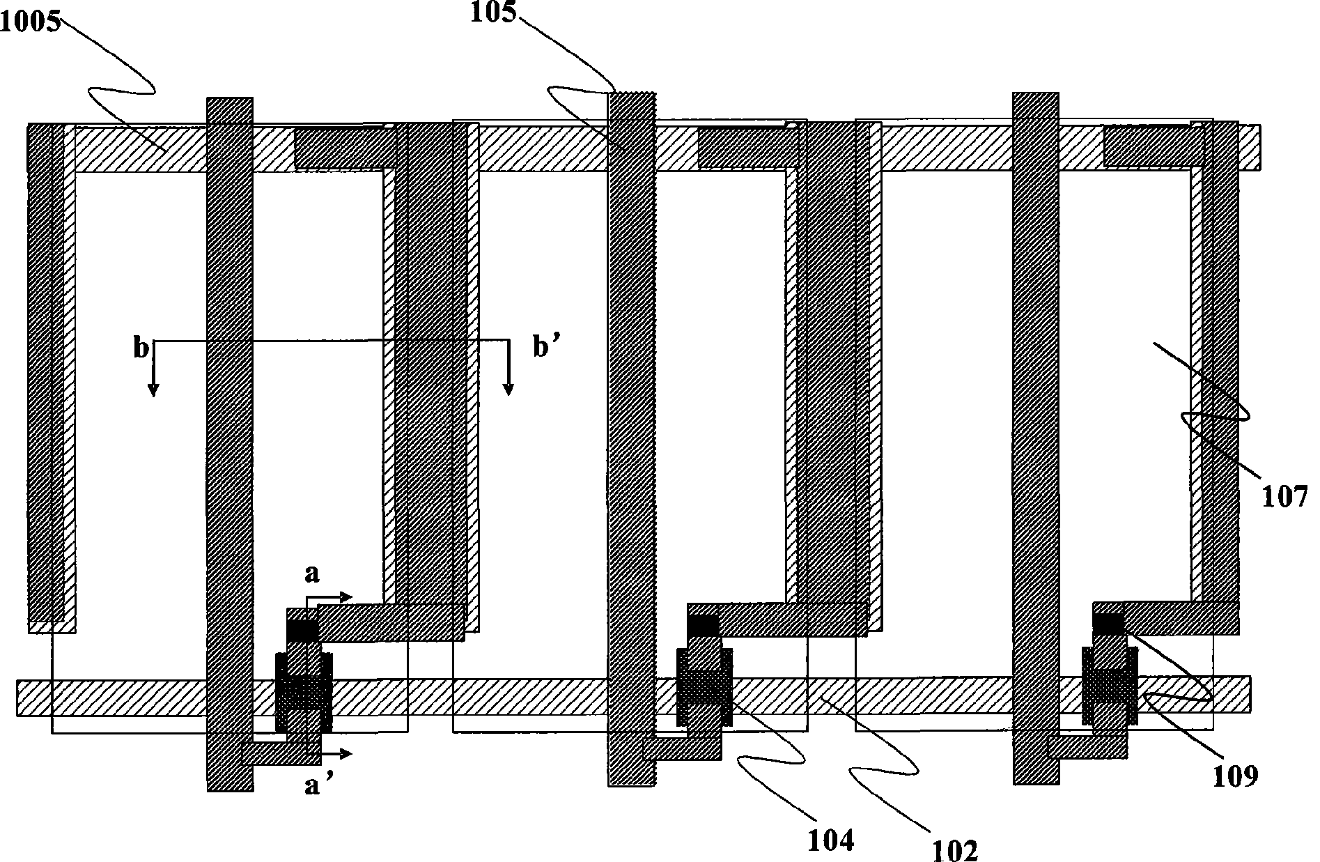
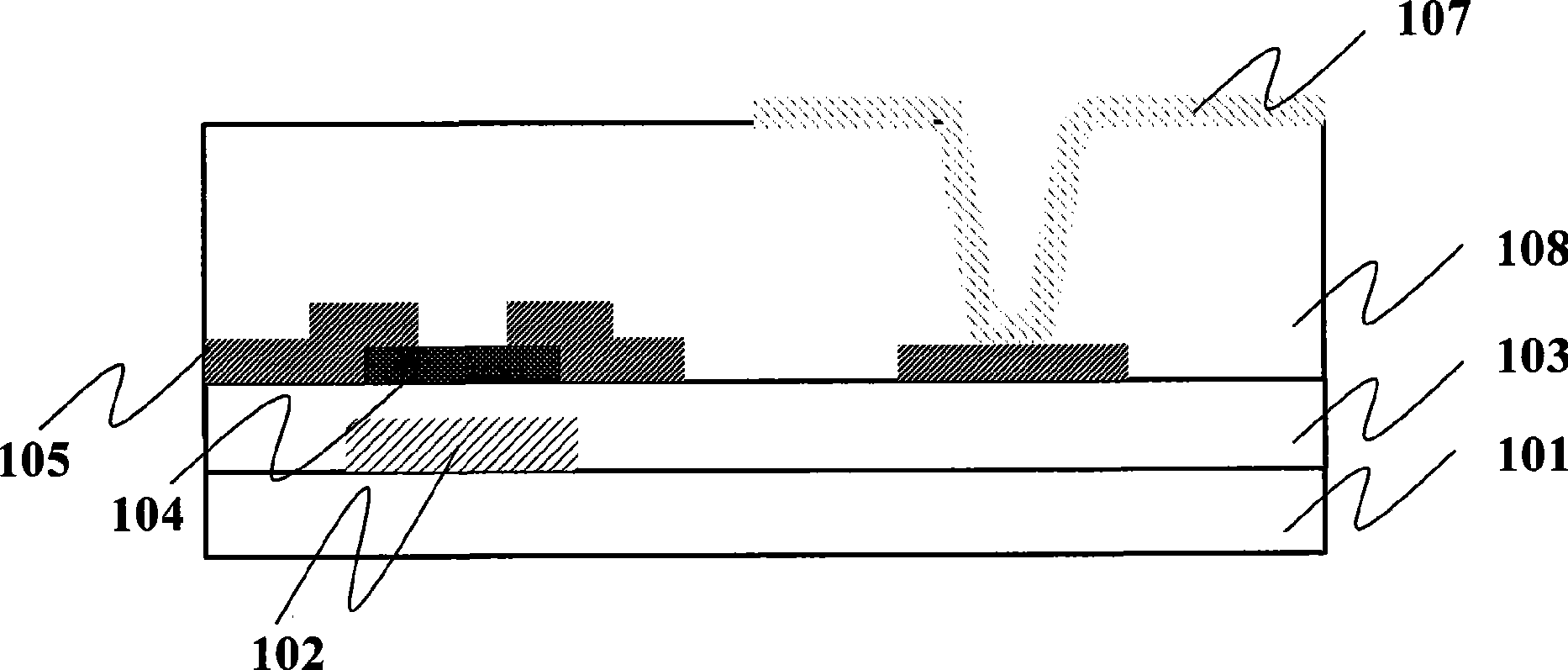
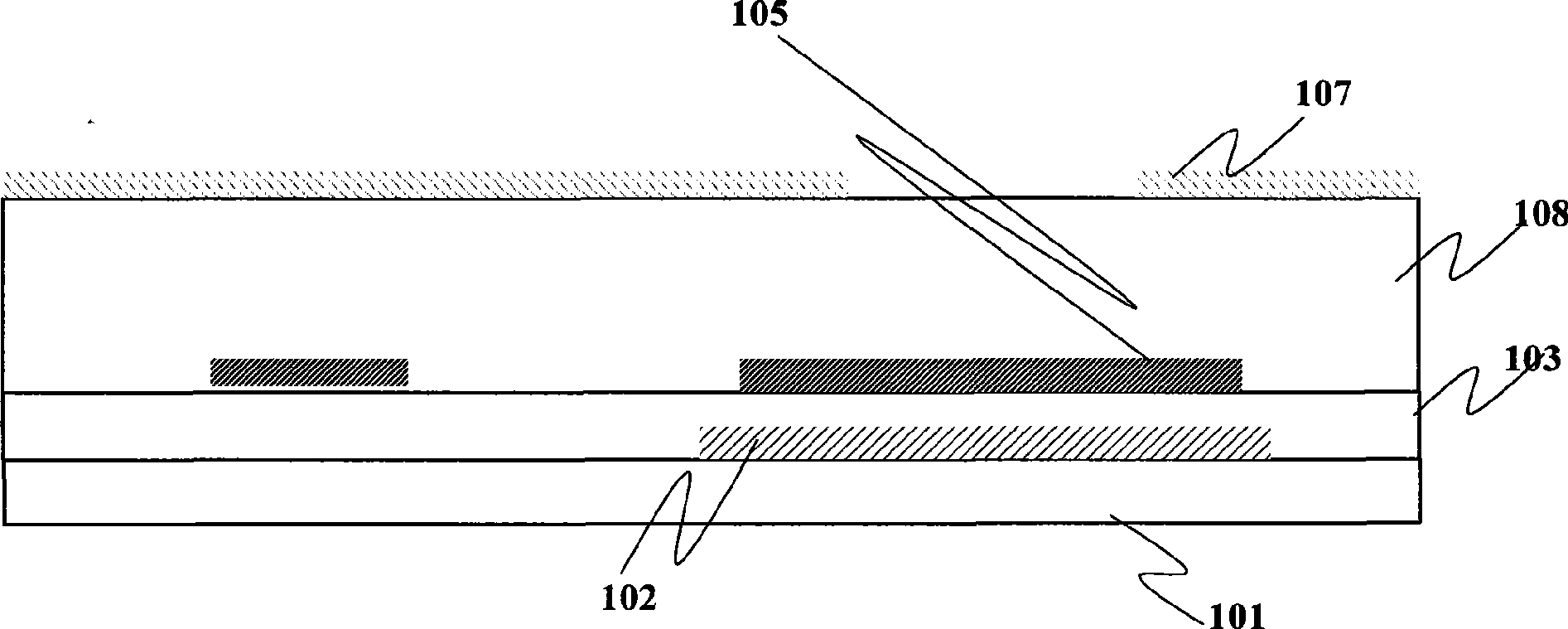
[0031] figure 1 It is a schematic diagram of the first embodiment of the liquid crystal display device of the present invention, figure 2 for along figure 1 The cross-sectional view of the a-a'direction, image 3 for along figure 1 The cross-sectional view of the b-b'direction. Such as figure 1 , figure 2 , image 3 As shown, the liquid crystal display device according to the first embodiment of the present invention mainly includes: a glass substrate 101, a gate scanning line layer 102 formed on the glass substrate 101, and a layer between the gate scanning line layer 102 and the active layer 104. An insulating layer 103, a data line layer 105, an insulating element 108, a pixel electrode layer 107, and a storage capacitor. Wherein, the insulating element is an organic insulating layer...


PUM


Abstract

The invention relates to a liquid crystal display device and a manufacture method thereof. The liquid crystal display device comprises a glass basic board as well as a grid scanning line layer, an insulating layer, a data line layer, a memory capacitance and a pixel electrode layer which are formed on the glass basic layer in sequence; wherein, the insulating layer is formed by overlapping an inorganic film and an organic film or an inorganic film with low specific inductive capacity or an organic film with low specific inductive capacity. The liquid crystal display device and a manufacture method thereof can improve the aperture opening ratio thereof, and reduce the signal delay of the data line or the grid scanning line.

Description

technical field [0001] The invention relates to a liquid crystal display device and a manufacturing method thereof, in particular to a liquid crystal display device capable of increasing the aperture ratio and a manufacturing method thereof. Background technique [0002] The traditional cathode ray tube (Cathode Ray Tube, CRT) display relies on the cathode ray tube to emit electrons and hit the phosphor powder on the screen to display images, while the principle of liquid crystal display (LCD) is completely different from that of CRT displays. Usually, liquid crystal display The device has an upper substrate and a lower substrate, which have a certain distance from each other and are facing each other. A plurality of electrodes formed on the two substrates are facing each other. The liquid crystal is sandwiched between the upper substrate and the lower substrate, and the voltage is applied through the electrodes on the substrate. to the liquid crystal, and then change the ar...

Claims


Application Information

Patent Timeline
Patent Type & Authority Applications(China)
IPC IPC(8): G02F1/1362G02F1/133H01L27/12H01L23/532H01L21/84H01L21/768
Inventor 秦锋
Owner SHANGHAI SVA LIQUID CRYSTAL DISPLAY
Why Eureka
Try Eureka