Semiconductor element structure and method for making the same

a semiconductor element and element structure technology, applied in the direction of semiconductor devices, electrical equipment, transistors, etc., can solve the problems of loss of electrical connection between the metal gates in the pmos and the nmos, inability to easily control the uniform thickness, and overly high electrical resistance. achieve the effect of stable and reliabl

Active Publication Date: 2009-08-20
MARLIN SEMICON LTD
View PDF4 Cites 16 Cited by
  • Summary
  • Abstract
  • Description
  • Claims
  • Application Information

AI Technical Summary

Benefits of technology

[0009]The present invention therefore provides a novel semiconductor element structure and a stable and reliable method to construct a sufficient electrical connection of the metal gates in the PMOS and the NMOS.

Problems solved by technology

Just after the deposition of the high-K materials and the metal gate materials, the electric connection between the metal gates in the PMOS and the NMOS is lost due to the isolation formed by the high-K materials.
Because, however, such a dishing space is too thin to be a suitable electrical connection as well as to be easily controlled and to stably and effectively maintain a sufficient electrical connection for the metal gates in the PMOS 101 and the NMOS 102, only an electrical connection with overly high electrical resistance is obtained.
Because, however, the back-etching is non-selective in the absence of a photoresist, the uniform thickness is not easily controlled and the height of the semiconductor device is compromised.

Method used


Image

  • Semiconductor element structure and method for making the same
  • Semiconductor element structure and method for making the same
  • Semiconductor element structure and method for making the same

Examples


Embodiment Construction

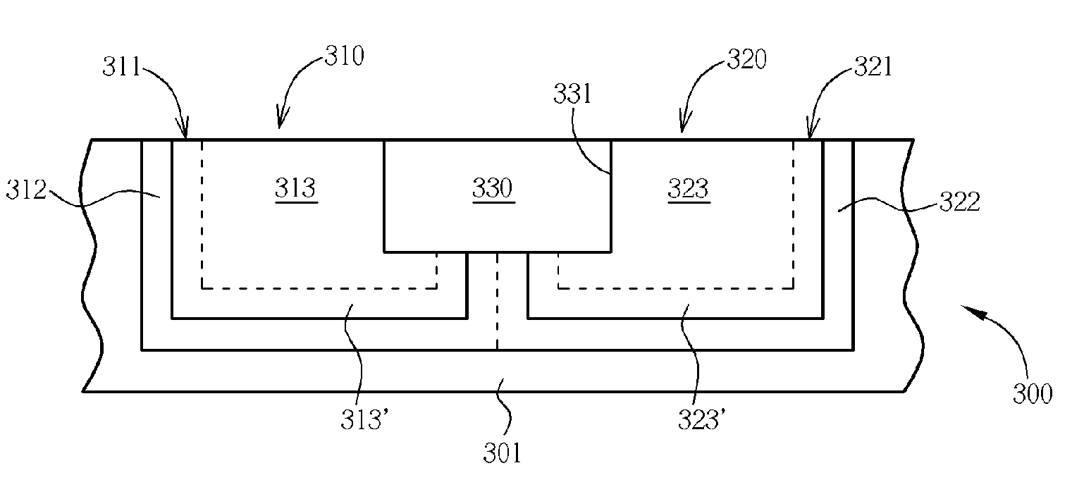
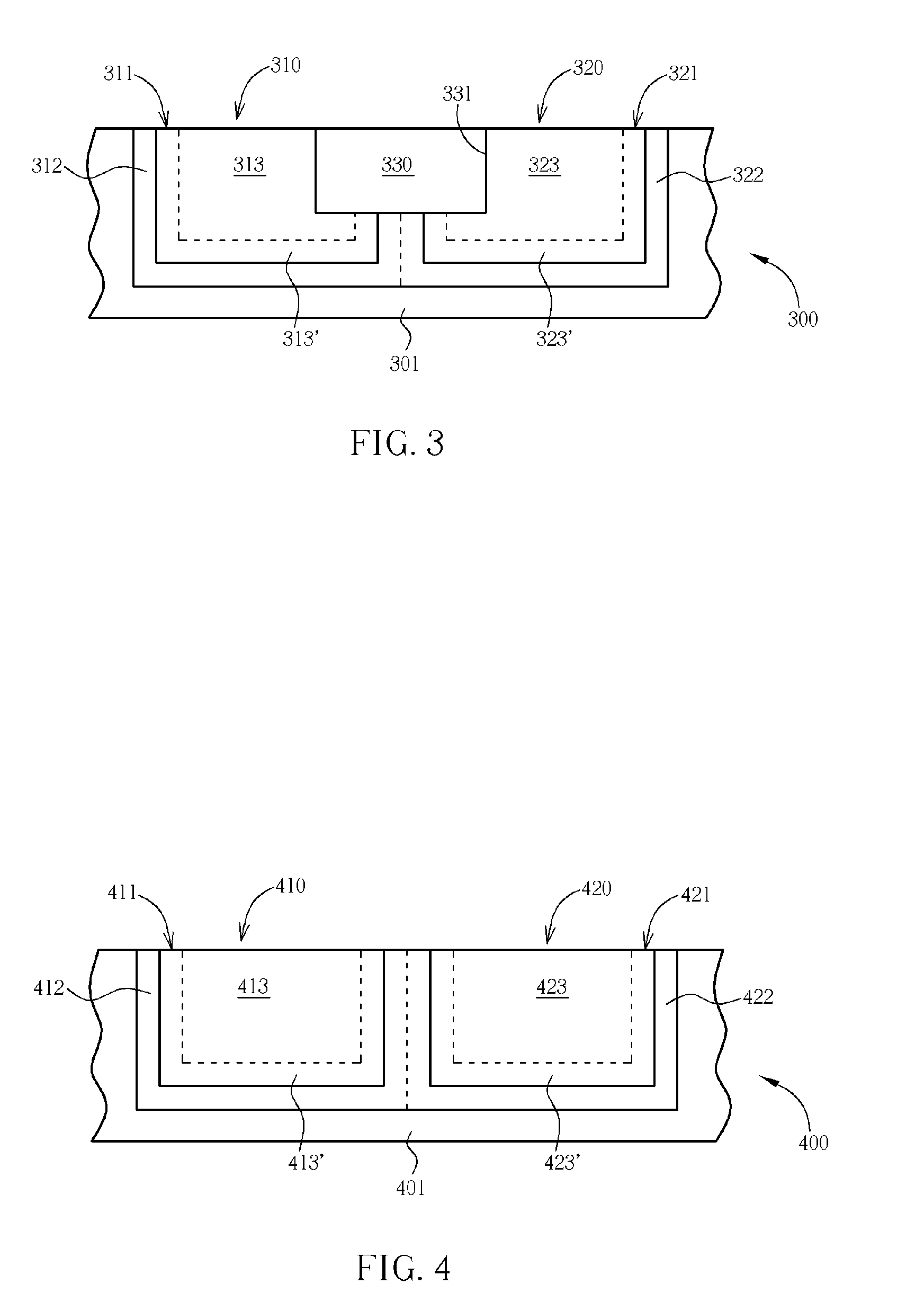
[0018]The present invention provides a novel inter-gate connecting structure for use in the invertors and SRAMs. The bridge channel therein not only does not change the height of the elements but also secures a sufficient electrical connection of each and every gate.

[0019]Please refer to FIG. 3, which illustrates a preferred embodiment of the present invention for use in the SRAMs. The semiconductor element structure 300 of the present invention includes a substrate 301, a first MOS 310, a second MOS 320 and a bridge channel 330. The first MOS 310 and the second MOS 320 respectively represent a PMOS and an NMOS and include any conventional elements, such as a source (not shown), a drain (not shown) and a gate. Please note that the assignment of the PMOS to the first MOS 310 and the NMOS to the second MOS 320 is arbitrary.

[0020]The first MOS 310 is disposed in the substrate 301 and includes a first high-K material 312 and a first metal 313 for a first gate 311. Similarly, the second ...


PUM


Abstract

A semiconductor element structure includes a first MOS having a first high-K material and a first metal for use in a first gate, a second MOS having a second high-K material and a second metal for use in a second gate and a bridge channel disposed in a recess connecting the first gate and the second gate for electrically connecting the first gate and the second gate, wherein the bridge channel is embedded in at least one of the first gate and the second gate.

Description

BACKGROUND OF THE INVENTION [0001]1. Field of the Invention[0002]The present invention relates to a semiconductor element structure and a method for forming the semiconductor element structure. More particularly, the present invention relates to a semiconductor element structure with an inter-gate bridge channel and a method for forming the semiconductor element structure.[0003]2. Description of the Prior Art[0004]The gate electrodes in a PMOS and NMOS of a static random access memory (SRAM) based on the complementary metal-oxide semiconductor (CMOS) structure are usually connected to each other. If such devices are manufactured by a high-K / metal gate replacement procedure, however, the poly-Si and the gate dielectric layer in the gates of the PMOS and the NMOS is removed in different steps to be replaced by the corresponding conductive metal gate and gate dielectric layer. Just after the deposition of the high-K materials and the metal gate materials, the electric connection betwee...

Claims


Application Information

Patent Timeline
Patent Type & Authority Applications(United States)
IPC IPC(8): H01L21/8238H01L27/092
CPCH01L21/823842H01L21/823871H01L27/11H01L29/66545H01L29/495H01L29/4966H01L29/517H01L27/1104H10B10/00H10B10/12
Inventor CHIANG, TIAN-FUCHENG, LI-WEIHSU, CHE-HUAYU, CHIH-HAOCHOULAI, CHIEN-MINGCHEN, YI-WENLIN, CHIEN-TINGMA, GUANG-HWA
Owner MARLIN SEMICON LTD
Why Eureka
Try Eureka