System and Method for Integrated Waveguide Packaging

a technology of integrated waveguide packaging and packaging system, which is applied in the manufacture of printed circuit components, printed circuit components, basic electric elements, etc., can solve the problems of inefficiency and high cost of serial manufacturing process that assembles only one millimeter wave package at a time, and can be relatively expensiv

Active Publication Date: 2009-08-20
VIASAT INC
View PDF5 Cites 32 Cited by
  • Summary
  • Abstract
  • Description
  • Claims
  • Application Information

AI Technical Summary

Problems solved by technology

Custom cast chassis and covers can be relatively expensive.
A serial manufacturing process that assembles only one millimeter wave package at a time can be inefficient and expensive.

Method used


Image

  • System and Method for Integrated Waveguide Packaging
  • System and Method for Integrated Waveguide Packaging
  • System and Method for Integrated Waveguide Packaging

Examples


Embodiment Construction

[0025]While exemplary embodiments are described herein in sufficient detail to enable those skilled in the art to practice the invention, it should be understood that other embodiments may be realized and that logical electrical and mechanical changes may be made without departing from the spirit and scope of the invention. Thus, the following detailed description is presented for purposes of illustration only.

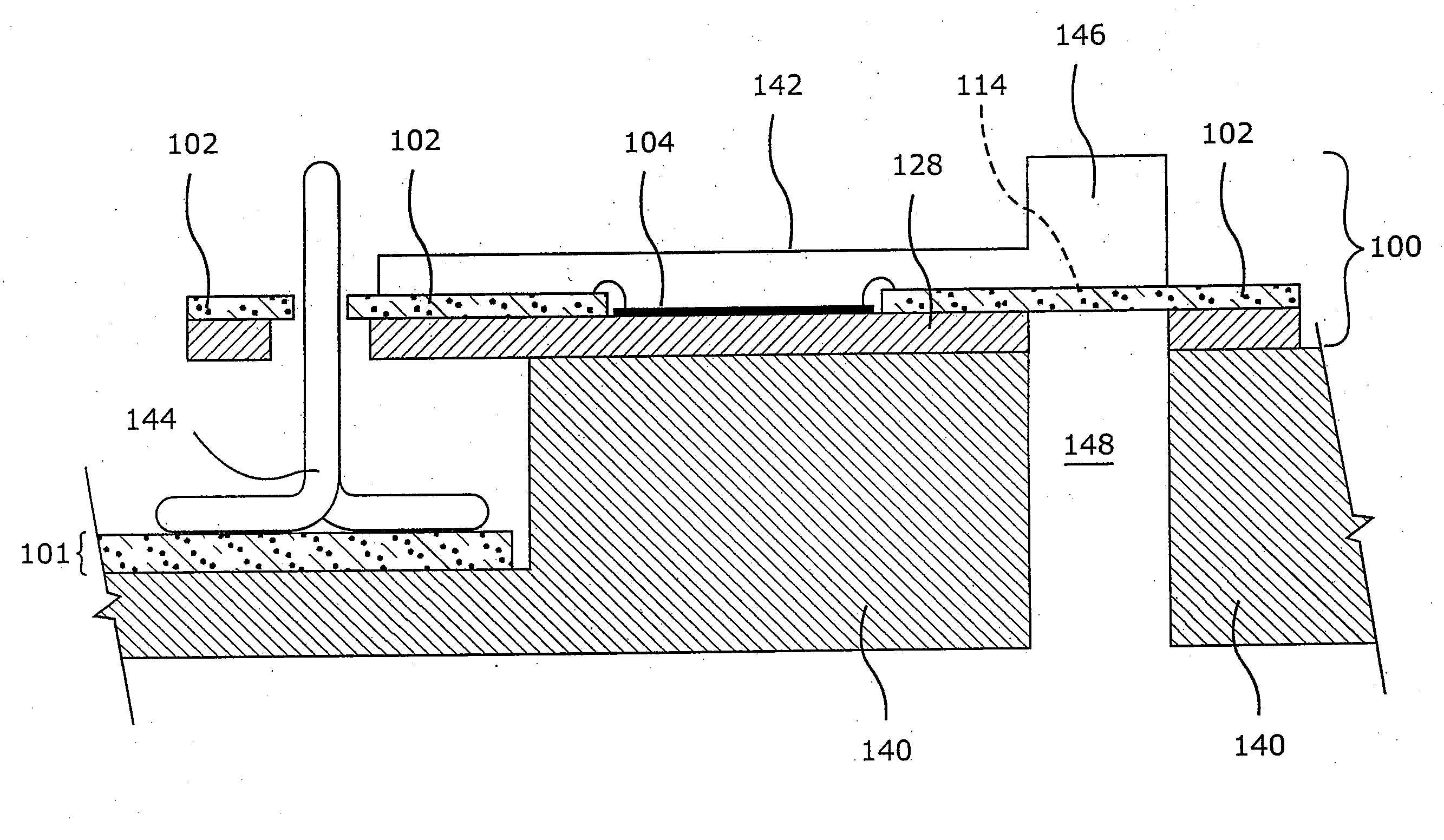
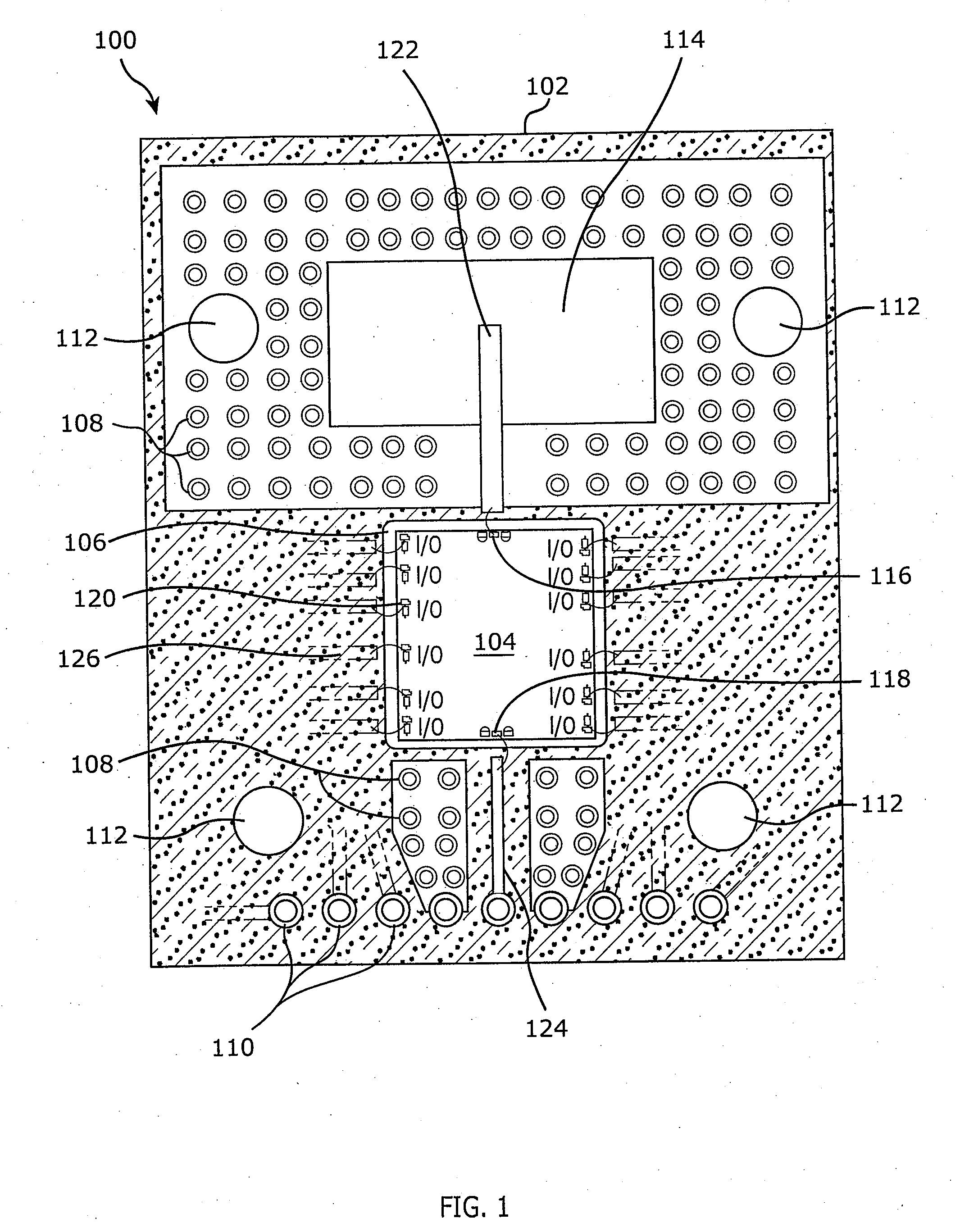
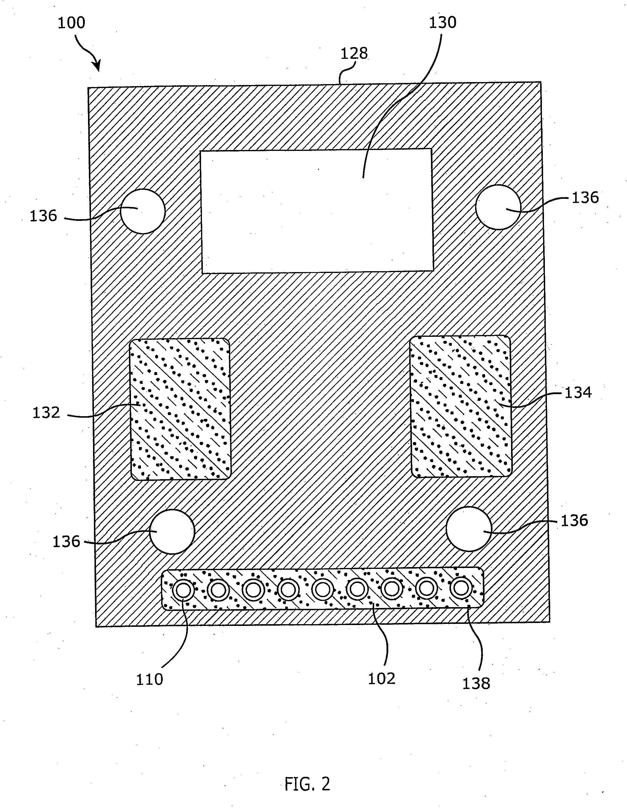
[0026]In accordance with an example of a millimeter waveguide package, and with reference to FIG. 1, a top view of a millimeter waveguide package 100 is shown with the radio frequency (RF) cover removed. The package 100 is an example of a reliable and low cost millimeter wave package, capable of being manufactured in parallel with other packages 100 in relatively high volumes, with desired microwave interfaces and thermal management. The package 100 includes a printed wiring board (PWB) 102 in communication with a monolithic microwave integrated circuit (MMIC) 104. PWB 102 inc...


PUM


Abstract

A millimeter wave system or package may include at least one printed wiring board (PWB), at least one integrated waveguide interface, and at least one monolithic microwave integrated circuit (MMIC). The package may be assembled in panel form incorporating parallel manufacturing techniques.

Description

FIELD OF INVENTION [0001]The present invention relates to millimeter wave packaging. More particularly, the invention relates to millimeter wave packaging manufactured using low cost and / or high yield techniques.BACKGROUND OF THE INVENTION [0002]Block up converters (BUCs), solid state power amplifiers (SSPAs), and similar systems are often employed in satellite communications systems to transmit and receive data by means of radio frequency (RF) signals. Many of these systems employ millimeter wave packaging including various components that provide needed functionality within the systems. For example, BUCs and SSPAs may comprise electrical and mechanical components such as monolithic microwave integrated circuits (MMICs), heat spreaders, printed wire boards (PWBs) or other similar structures, waveguides, chassis, RF covers, and / or various other components. Such components cooperate to reliably process RF signals in a productive manner consistent with the purposes of the particular s...

Claims


Application Information

Patent Timeline
Patent Type & Authority Applications(United States)
IPC IPC(8): H01L23/66H01L21/58
CPCH01L23/13H01L2224/48227H01L23/66H01L24/28H01L24/48H01L24/85H01L24/97H01L2223/6633H01L2224/2919H01L2224/48091H01L2224/49175H01L2224/97H01L2924/01013H01L2924/01027H01L2924/01029H01L2924/0103H01L2924/01074H01L2924/01078H01L2924/01079H01L2924/01082H01L2924/14H01L2924/1423H01L2924/15153H01L2924/1517H01L2924/1616H01L2924/19039H01L2924/19041H01L2924/19043H01L2924/19105H01L2924/30107H05K1/0203H05K1/0243H05K3/0061H05K2201/09845H05K2201/10189H01L23/4006H01L2224/85H01L2924/01033H01L24/49H01L2924/00014H01L2924/0665H01L2924/3512H01L2924/00H01L2224/45099H01L2224/45015H01L2924/207
Inventor LOPEZ, NOEL A.LYONS, MICHAEL R.LAIDIG, DAVEBUER, KENNETH V.
Owner VIASAT INC
Why Eureka
Try Eureka