Method of manufacturing liner for semiconductor processing chamber, liner and chamber including the liner

a manufacturing method and technology for semiconductors, applied in manufacturing tools, mechanical vibration separation, coatings, etc., can solve the problems of contaminants adhering to the liners, deposited materials have the potential of peeling, and the potential of reappearing in the plasma as undesired components,

Inactive Publication Date: 2009-08-20
B&H ENG
View PDF8 Cites 24 Cited by
  • Summary
  • Abstract
  • Description
  • Claims
  • Application Information

AI Technical Summary

Problems solved by technology

If they are deposited other than on the intended substrate or wafer, the deposited material have the potential of peeling off and landing on the wafer as contamination or re-entering the process gases as contamination.
They also have the potential of reappearing in the plasma as undesired components.
The contaminants adhere to the liners.

Method used


Image

  • Method of manufacturing liner for semiconductor processing chamber, liner and chamber including the liner
  • Method of manufacturing liner for semiconductor processing chamber, liner and chamber including the liner
  • Method of manufacturing liner for semiconductor processing chamber, liner and chamber including the liner

Examples


Embodiment Construction

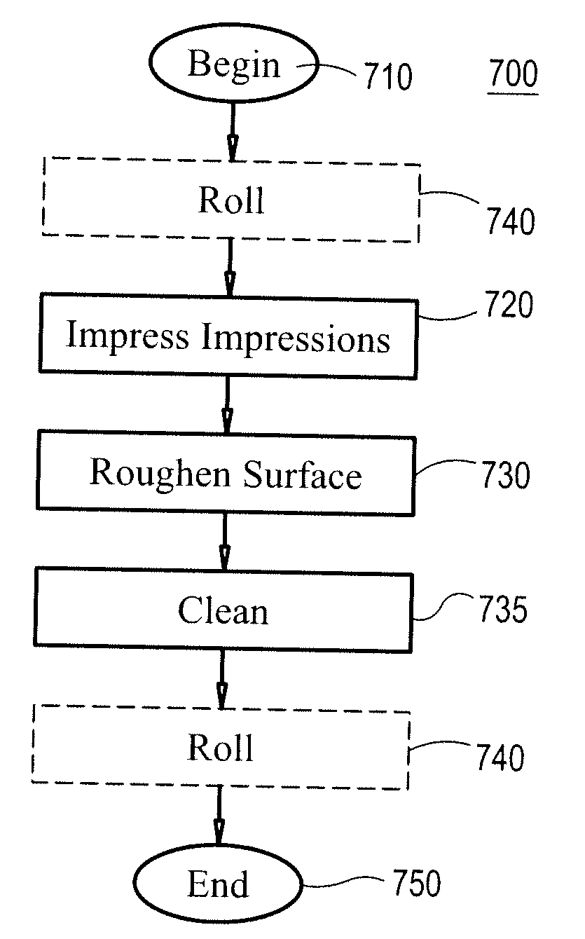
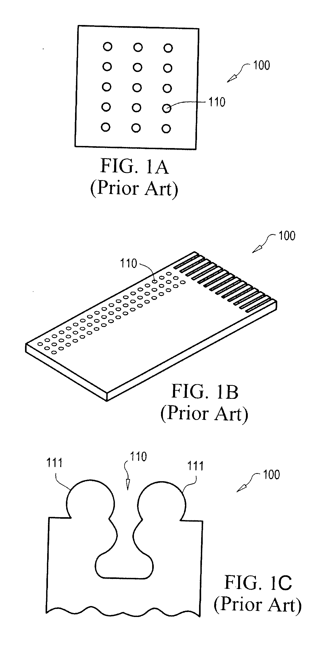
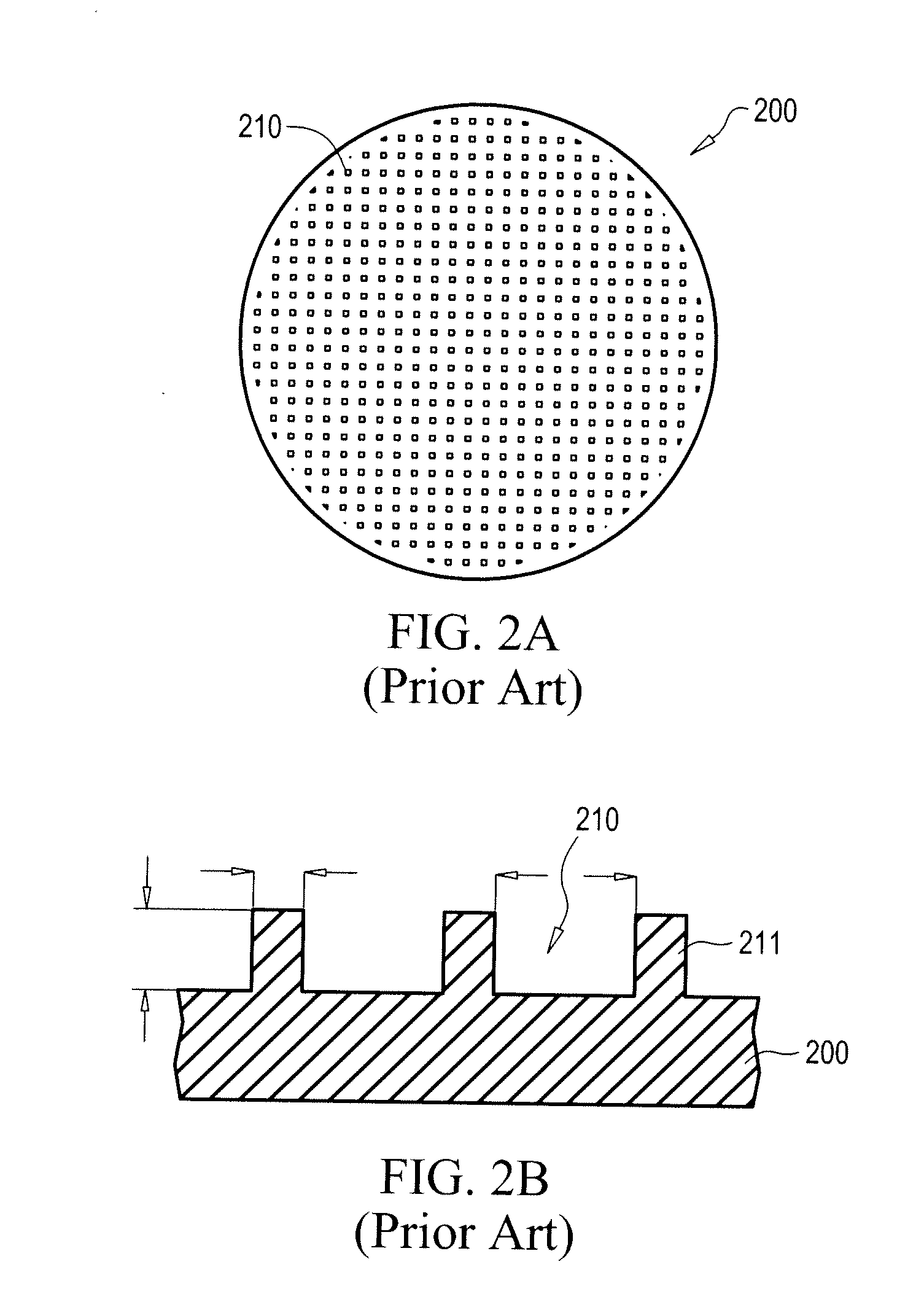
[0044]The potential for contamination of chamber by material deposited on the walls of the chamber may be reduced by improving the adhesion between the walls and the material within the processing chamber that are deposited on the walls. This material may be atoms being carried by the plasma, process gases, polymers, or particulates floating within the chamber.

[0045]Alternatively, a liner may be added to line the internal walls of the processing chamber. Then, this liner may be manufactured to have improved adhesion with the material in the plasma within the plasma chamber. A liner may alternatively be called a shield. A shield is said to shield the walls of the process chamber.

[0046]When the thickness of the layer of contamination increases beyond a limit, the adhesivity between the liner material and the contamination layer is no longer sufficient to hold the contamination attached to the liner. Thermal cycling occurring in the chamber causes flaking of the material adhering to th...


PUM

PropertyMeasurementUnit
thicknessaaaaaaaaaa
diameteraaaaaaaaaa
thicknessaaaaaaaaaa

Abstract

A method for manufacturing a liner for a process chamber, a liner and a process chamber including the liner. A surface of a liner material is impressed with impressions by pressing, punching, dimpling, embossing, drilling, knurling or otherwise mechanically altering the surface without removing material. The impressions include depressions, protuberances, or a combination of depressions and protuberances that are separate or merge together. The impressions may be formed as one group or as two consecutive groups and may have different shapes and arrangement patterns. The surface may be roughened before or after forming the impressions. The roughening may be obtained from particulate blasting, plasma spray, and arc spray. The sheet of material may be aluminum, steel, an alloy or a composite material that is capable of being impressed by pressing or punching. The liner may be disposable or may be cleaned after a certain number of usage cycles.

Description

BACKGROUND OF THE INVENTION[0001]1. Field of the Invention[0002]This invention relates to chambers for processing semiconductors and, more particularly, to liners used in semiconductor process chambers.[0003]2. Description of the Related Art[0004]Semiconductor processing, for example processing of semiconductor wafers to form integrated circuits (IC), is usually performed in several stages. Some stages and types of semiconductor processing are performed in semiconductor processing chambers. These types of processing may include physical vapor deposition (PVD), chemical vapor deposition (CVD), plasma etch processes, ion metal plasma (IMP), atomic layer deposition (ALD), ion implantation, annealing and the like. In most of these processes, a substrate is exposed to one or more gas-phase materials. For example, in the PVD and CVD processes, atoms of a target material are deposited on a substrate such as a semiconductor wafer. In plasma etching the wafer is etched away by being bombarde...

Claims


Application Information

Patent Timeline
Patent Type & Authority Applications(United States)
IPC IPC(8): B29C71/00B29C59/02B05C11/00
CPCC23C16/4404C23C14/564
Inventor BEGOVIC, BAKIR
Owner B&H ENG
Why Eureka
Try Eureka