Lamella structured thin films with ultralow dielectric constants and high hardness and method for manufacturing the same

Inactive Publication Date: 2009-08-20
RES & BUSINESS FOUNDATION SUNGKYUNKWAN UNIV
View PDF0 Cites 2 Cited by
  • Summary
  • Abstract
  • Description
  • Claims
  • Application Information

AI Technical Summary

Benefits of technology

[0032]In the conventional silica thin film, in order to reduce the dielectric constant, the ratio of pores is to be increased, which deteriorates the mechanical strength of the thin film. On the other hand, according to the present invention, since it is possible to reduce the dielectric constant lower than that of the conventional silica thin film while reducing the ratio of the pores, the mechanical strength of the thin film does not significantly deteriorate. Also, since the lamella structured thin film itself represents the effect of increasing the hardness, the hardness of the film increases.
[0033]Therefore, it is possible to provide thin films having ultralow dielectric constants and high mechanical strength simultaneously, which the prior arts could not achieve. Therefore, the present invention provides structure that can solve the two problems and a method of manufacturing actually usable materials.
[0034]In the conventional porous low dielectric constant thin films, the pores a

Problems solved by technology
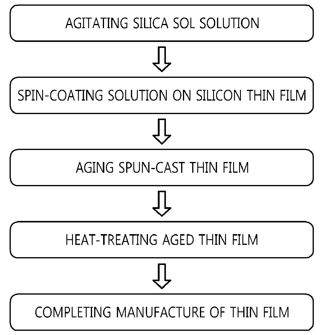
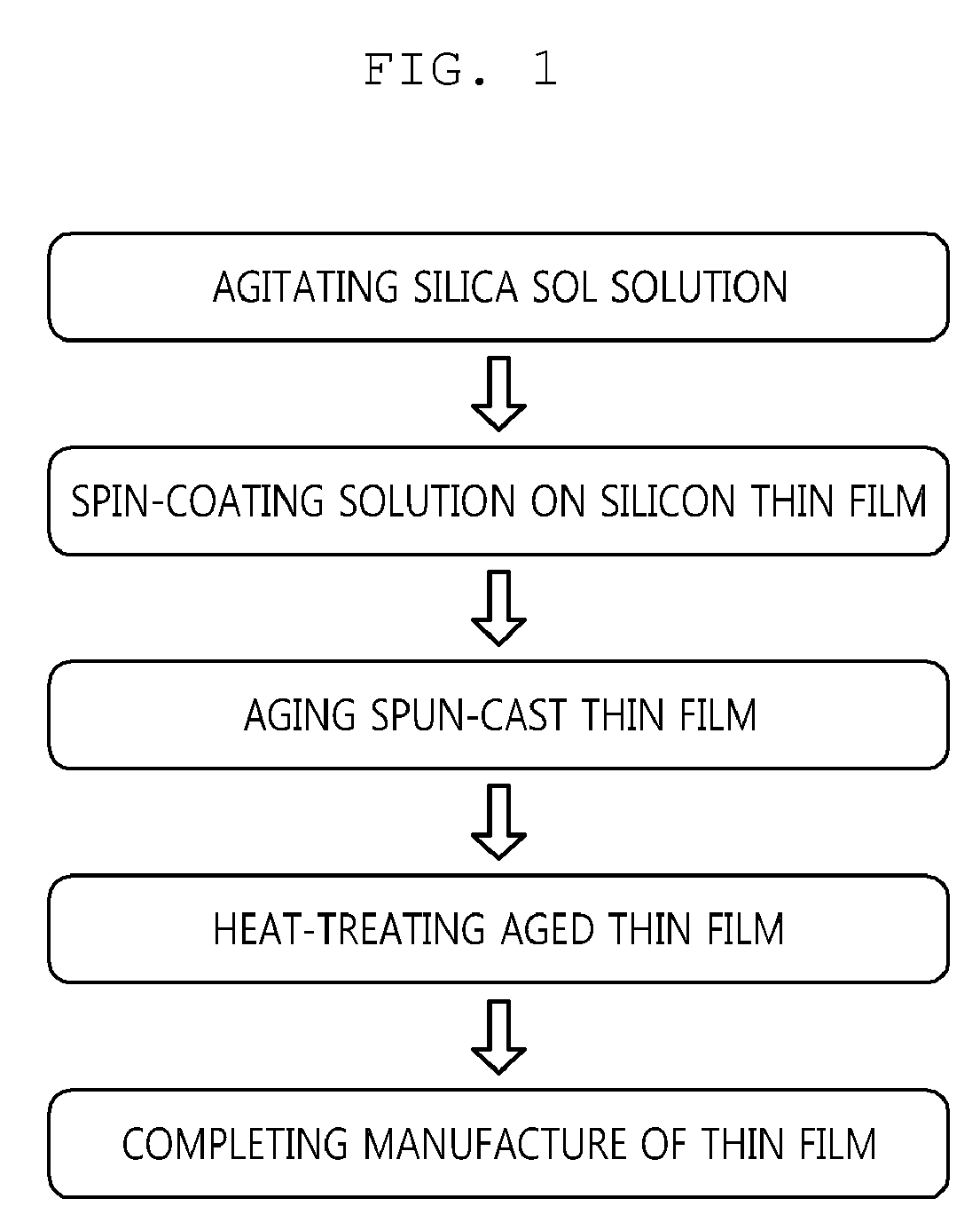
However, the dielectric constant of the silicon dioxide (SiO2) film is about 4, which is too high to be used as the next generation chip-to-chip package material that particularly requires low dielectric constant.
However, in order to reduce the die

Method used


Image

  • Lamella structured thin films with ultralow dielectric constants and high hardness and method for manufacturing the same
  • Lamella structured thin films with ultralow dielectric constants and high hardness and method for manufacturing the same
  • Lamella structured thin films with ultralow dielectric constants and high hardness and method for manufacturing the same

Examples


Example

Comparative Embodiment 1

[0075]SiLK as low dielectric constant material was manufactured by a spin-coating method using a polymer and an organic solvent described in the reference document (Adv. Mater. 2000, 12, 1769). However, the dielectric constant of the material is 2.65, the Young's modulus of the material is 2.45 GPa, and the hardness of the material is 0.38 GPa. Therefore, it is noticed that the material of the comparative embodiment 1 has a significantly higher dielectric constant and significantly lower Young's modulus and hardness than those of the present invention. Therefore, it was noticed that the films of the present invention have significantly higher performance than conventional low dielectric constant materials.

Example

Comparative Embodiment 2

[0076]In accordance with the reference document (Chem. Mater. 2002, 14, 1845-1852), low dielectric constant thin film having mesopores was manufactured by a spin-coating method using a silica source based on hydrogen silsesquioxane and a solvent having low boiling point such as methylpropyl ketone.

Example

Comparative Embodiment 3

[0077]In accordance with the reference document (Langmuir 2001, 17, 6683-6691), low dielectric constant thin film was manufactured by a spin-coating method using PMSSQ / BTMSE prepolymer, Bis(1,2-trimethoxysilyl)ethane (BTMSE), and methyltrimethoxysilane (MSSQ).

[0078]As a result of measuring the dielectric constants of the thin films generated by the comparative embodiments 1 to 3, it was noticed that the dielectric constants were about 2.5 to 3.5, which are significantly larger than the dielectric constants of the films manufactured by the method of the present invention.

[0079]As described above, the lamella structured thin film according to the present invention has excellent mechanical strength and chemical stability, in particular, have significantly low dielectric constant of no more than 2.5 and high hardness. In addition, according to the method for manufacturing the lamella structured thin film of the present invention, the semiconductor manufacturing p...


PUM


Abstract

There are provided lamella structured thin films having ultralow dielectric constants and high hardness, and the method for manufacturing the same. In the lamella structured thin film, silica layers and air layers are alternately and repeatedly stacked on the surface of a wafer in the vertical direction. The method of manufacturing the lamella structured thin film includes, agitating silica sol solution containing surfactant and silica precursor, spin-coating the solution on silicon wafer, aging the wafer, and annealing the wafer to remove the surfactant and organic materials from the wafer. The lamella structured thin film has excellent mechanical strength and high chemical stability, and in particular, has significantly low dielectric constant of no more than 2.5 and high hardness. In the method of manufacturing the lamella structured thin film, semiconductor processes can be made simple and economical since only pure silica is used and no additionally surface treatment is performed.

Description

BACKGROUND OF THE INVENTION[0001]1. Field of the Invention[0002]The present invention relates to lamella structured thin films having ultralow dielectric constants (K) and high hardness and a method of manufacturing the same.[0003]2. Description of the Background Art[0004]Recently, researches on new materials having low dielectric constant are actively performed since the low dielectric constant material is required for reducing the feature dimension of an integrated circuit to improve the degree of integration. The silicon dioxide (SiO2) film has been the material of choice for the conventional semiconductor packaging and the interlayer insulating material. However, the dielectric constant of the silicon dioxide (SiO2) film is about 4, which is too high to be used as the next generation chip-to-chip package material that particularly requires low dielectric constant.[0005]On the other hand, several researchers have sought solutions to the problems of silicon dioxide from nanoporous...

Claims


Application Information

Patent Timeline
IPC IPC(8): B32B7/02H01L21/31
CPCH01L21/3121Y10T428/265H01L21/7682H01L21/316H01L21/02126H01L21/02164H01L21/02203H01L21/02216H01L21/02282H01L21/02211H01L27/13
Inventor KWON, YOUNG UKLEE, U. HWANGLEE, HYUN JULEE, KI RIM
Owner RES & BUSINESS FOUNDATION SUNGKYUNKWAN UNIV
Why Eureka
Try Eureka