

Resistor triggered electrostatic discharge protection
a resistor and electrostatic discharge technology, applied in the direction of diodes, transistors, electrical apparatuses, etc., can solve the problems of modern electronic devices, especially semiconductor devices and integrated circuits (ics), at risk of damag
- Summary
- Abstract
- Description
- Claims
- Application Information
AI Technical Summary
Problems solved by technology
Method used
Image

Examples
first embodiment
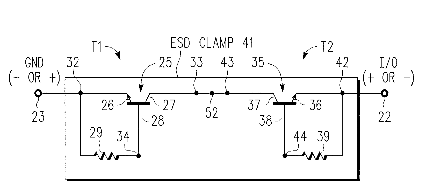
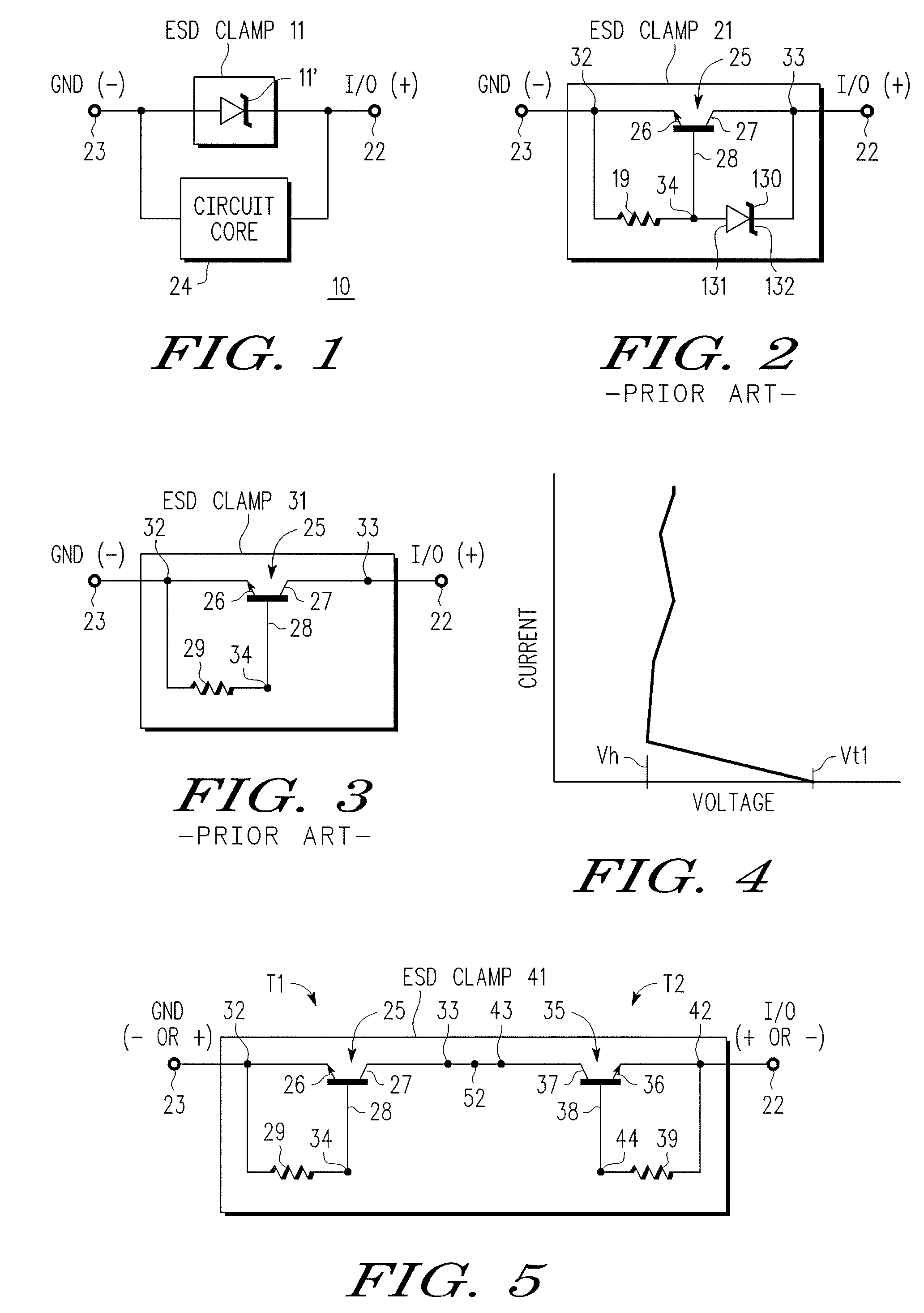
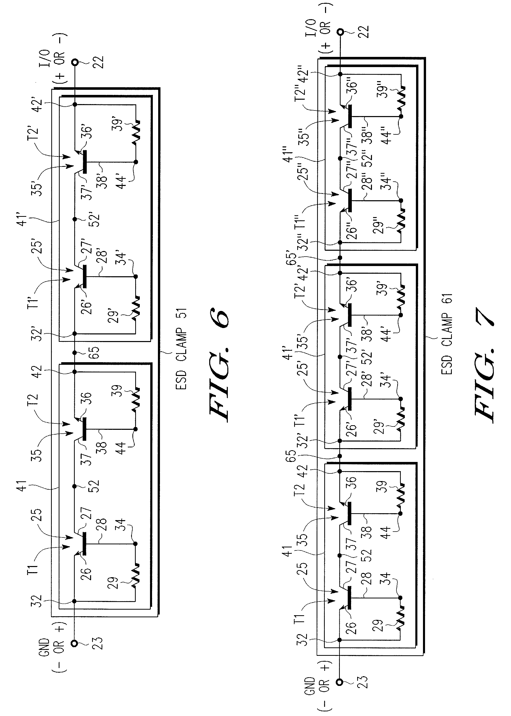
[0031] there is provided an electronic device having input / output (I / O) and common terminals, comprising, a circuit core coupled between the I / O and common terminals, and one or more serially arranged resistor triggered bi-directional ESD clamp stages coupled between the I / O and common terminals. According to a further embodiment, there is only one resistor triggered bi-directional ESD clamp stage. According to a still further embodiment, each resistor triggered bi-directional ESD clamp stage comprises first and second serially coupled bipolar transistors, each bipolar transistor having an emitter, a base and a collector, and wherein the emitter of the first transistor is coupled to the common terminal and the emitter of the second transistor is coupled to the I / O terminals and the collectors of the first and second transistors are coupled together, and a first external resistor is coupled between the emitter and base of the first transistor and a second external resistor is coupled...
second embodiment
[0032] there is provided an integrated ESD protection device, having I / O and common terminals adapted to be coupled to I / O and common terminals of a core circuit being protected by the integrated ESD protection device, comprising, first and second bipolar transistors having a common collector region and comprising, first and second base regions of a first conductivity type, one base region for each bipolar transistor, a region of a second, opposite conductivity type extending beneath the first and second base regions, and separating and laterally surrounding the first and second base regions, and serving as the common collector region of the first and second bipolar transistors, a first emitter region of the second conductivity type within the first base region and a second emitter region of the second conductivity type within the second base region, wherein the first emitter region is adapted to be coupled to the common terminal of the core circuit and the second emitter region is ...
third embodiment
[0033] there is provided an ESD protection device adapted to be coupled between common and I / O terminals of a core circuit desired to be protected, comprising, one or more bi-directional resistor triggered ESD stages, each stage comprising, two bipolar transistors having a common collector and isolation region, a base region for each transistor separated by a portion of the common collector and isolation region, separate emitter regions, one in each base region, base contact regions, one for each base region, and ESD trigger resistors external to the transistors, coupled between the emitter region and the base contact region of each transistor. According to a still further embodiment, the ESD trigger resistors lie laterally outside the collector and isolation region. According to a still further embodiment, the ESD trigger resistors are thin film resistors. According to a yet further embodiment, the ESD trigger resistors have resistance values in the range of about 0.5 k Ohms to 150...
PUM
 Abstract
Description
Claims
Application Information