
Methods of manufcturing a semiconductor device

a manufacturing method and semiconductor technology, applied in the direction of semiconductor devices, basic electric elements, electrical appliances, etc., can solve the problems of reducing device performance, affecting device performance, and thereby limited device performance, so as to improve electrical characteristics

Active Publication Date: 2009-09-10
SAMSUNG ELECTRONICS CO LTD
View PDF7 Cites 17 Cited by
  • Summary
  • Abstract
  • Description
  • Claims
  • Application Information

AI Technical Summary

Benefits of technology

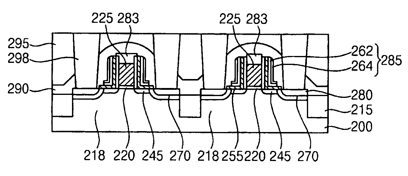
[0023]According to the example embodiments, stress may be concentrated on a channel and junction leakage may not occur adjacent to a source / drain region. Thus, a semiconductor device may have improved electrical characteristics.

Problems solved by technology

However, because cobalt and / or nickel are to be formed in a thin layer when used as a silicide layer, these configurations have encountered processing difficulties.
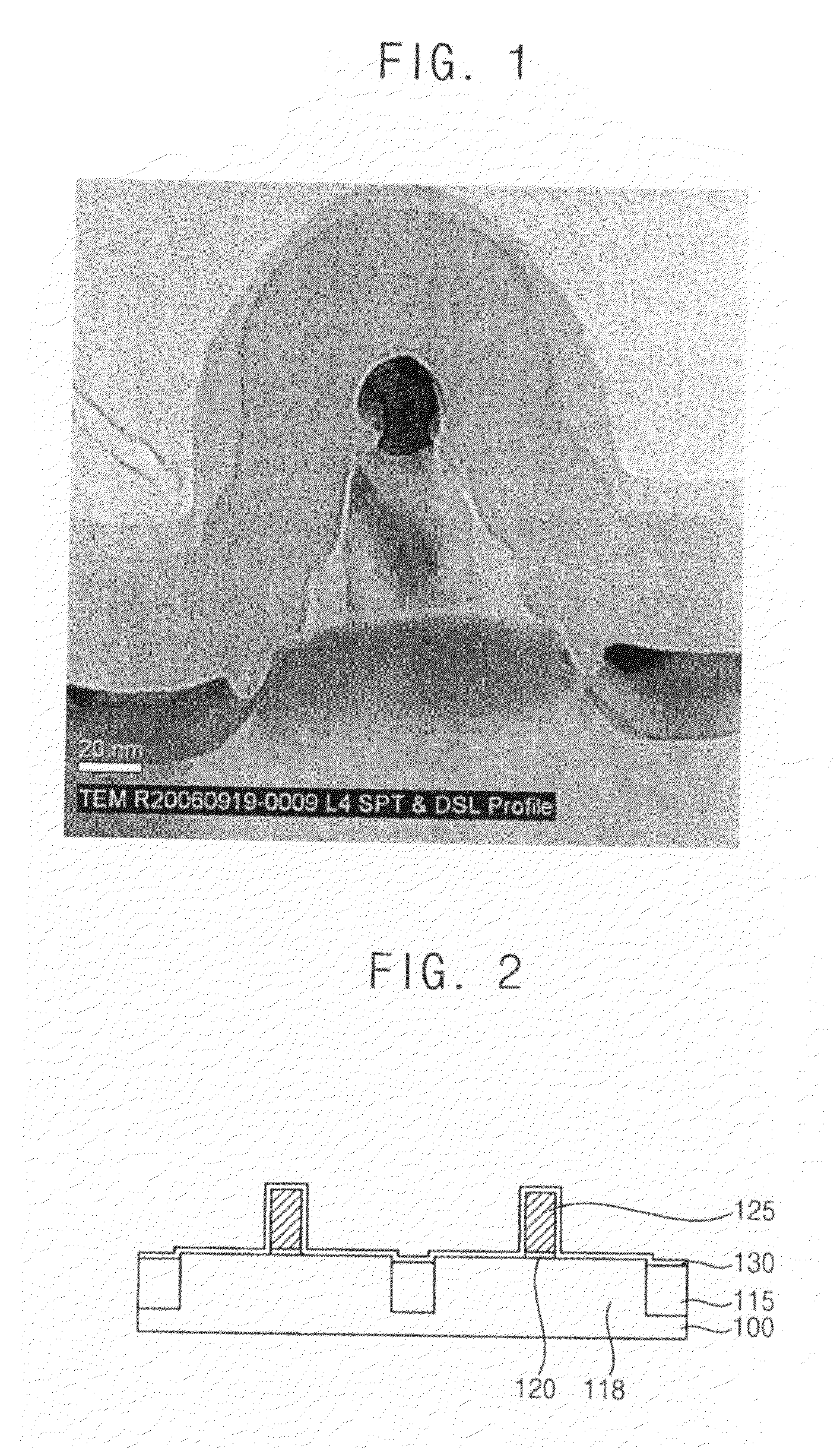
However, when the gate spacer is removed by a dry etching process, the active region may be attacked by the etch, causing the source / drain region to become over-etched, which can result in junction leakage during operation, and therefore reducing device performance.
In this case, an active region can become over-etched during removal of the gate spacer, and device performance can be thereby limited.

Method used


Image

  • Methods of manufcturing a semiconductor device
  • Methods of manufcturing a semiconductor device
  • Methods of manufcturing a semiconductor device

Examples


Embodiment Construction

[0028]This application claims priority under 35 USC §119 to Korean Patent Application No. 10-2008-0021967, filed on Mar. 10, 2008 in the Korean Intellectual Property Office (KIPO), the contents of which are herein incorporated by reference in their entirety.

[0029]Various example embodiments will be described more fully hereinafter with reference to the accompanying drawings, in which some example embodiments are shown. The present invention may, however, be embodied in many different forms and should not be construed as limited to the example embodiments set forth herein. Rather, these example embodiments are provided so that this disclosure will be thorough and complete, and will fully convey the scope of the present invention to those skilled in the art. In the drawings, the sizes and relative sizes of layers and regions may be exaggerated for clarity.

[0030]It will be understood that when an element or layer is referred to as being “on,”“connected to” or “coupled to” another eleme...


PUM


Abstract

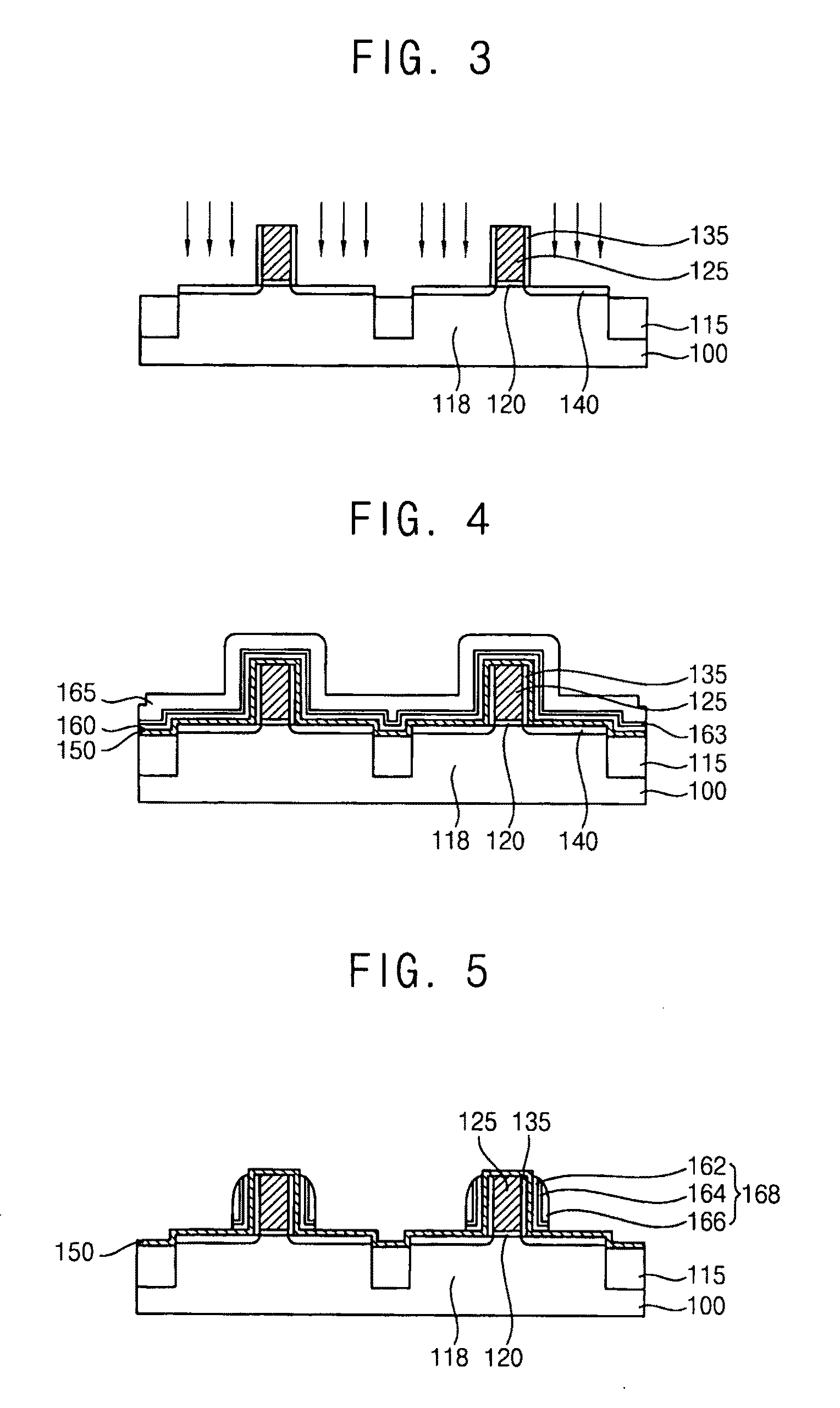
Isolation regions are formed on a substrate to define an active region. A gate electrode is formed on the active region. A spacer structure is formed on a sidewall of the gate electrode. A gate silicide layer is formed on the gate electrode and a source / drain silicide layer is formed on the active region adjacent to the gate electrode. An upper portion of the gate silicide layer and a portion of the spacer structure are simultaneously removed to form a spacer structure pattern and a gate silicide layer pattern. A stress layer is formed to cover the gate electrode and spacer structure pattern.

Description

BACKGROUND[0001]1. Field[0002]Example embodiments relate to a method of manufacturing a semiconductor device. More particularly, example embodiments relate to a method of manufacturing a semiconductor device having a metal silicide layer.[0003]2. Description of the Related Art[0004]Semiconductor devices commonly employ switching devices such as a metal-oxide semiconductor (MOS) transistors. As the degree of integration of semiconductor devices continues to increase, the size of MOS transistors continues to decrease. Accordingly, the channel length of the MOS transistor is reduced, and, as a result, the occurrence of the short channel effect is more likely. Also, the resulting width of a gate electrode may be reduced due to the reduction of the channel length of the MOS transistor. As a result, the electrical resistance of the gate electrode may be increased.[0005]A silicidation process for decreasing the electrical resistance of semiconductor devices is widely employed. Generally, t...

Claims


Application Information

Patent Timeline
Patent Type & Authority Applications(United States)
IPC IPC(8): H01L21/76
CPCH01L21/823807H01L29/7843H01L21/823864H01L21/823814H01L21/24
Inventor SHIN, DONG-SUKKIM, KI-CHULLEE, JUNG-DEOG
Owner SAMSUNG ELECTRONICS CO LTD
Learn More