Optical device manufacturing method

a manufacturing method and optical device technology, applied in the direction of manufacturing tools, after-treatment details, semiconductor lasers, etc., can solve the problems of poor productivity, difficult to simultaneously cut high-brittle optical device wafers and heat sink materials made of metal such as high-ductile copper, and achieve the effect of efficient manufacturing

a manufacturing method and optical device technology, applied in the direction of manufacturing tools, after-treatment details, semiconductor lasers, etc., can solve the problems of poor productivity, difficult to simultaneously cut high-brittle optical device wafers and heat sink materials made of metal such as high-ductile copper, and achieve the effect of efficient manufacturing

US20090233419A1Active Publication Date: 2009-09-17DISCO CORP

Image

  • Optical device manufacturing method
  • Optical device manufacturing method
  • Optical device manufacturing method

Examples


Embodiment Construction

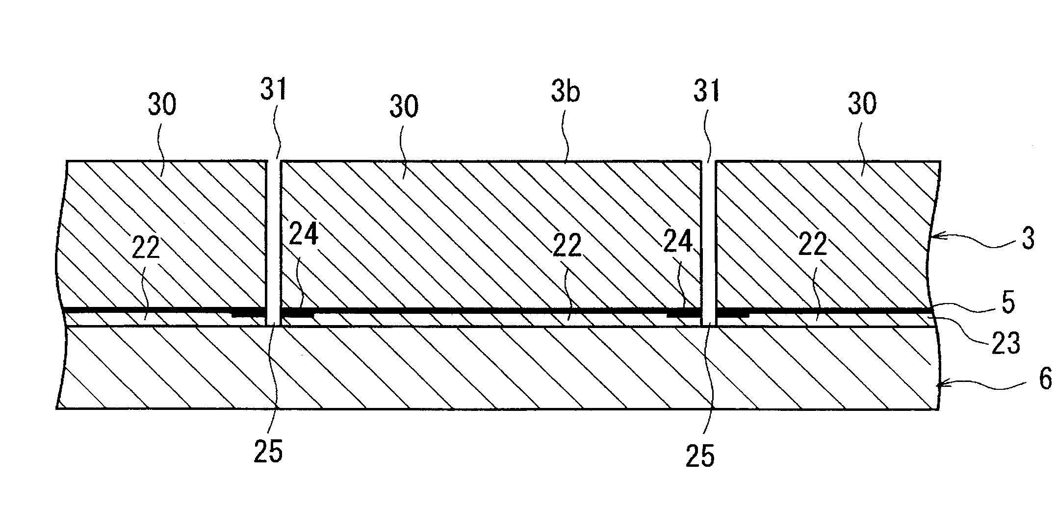
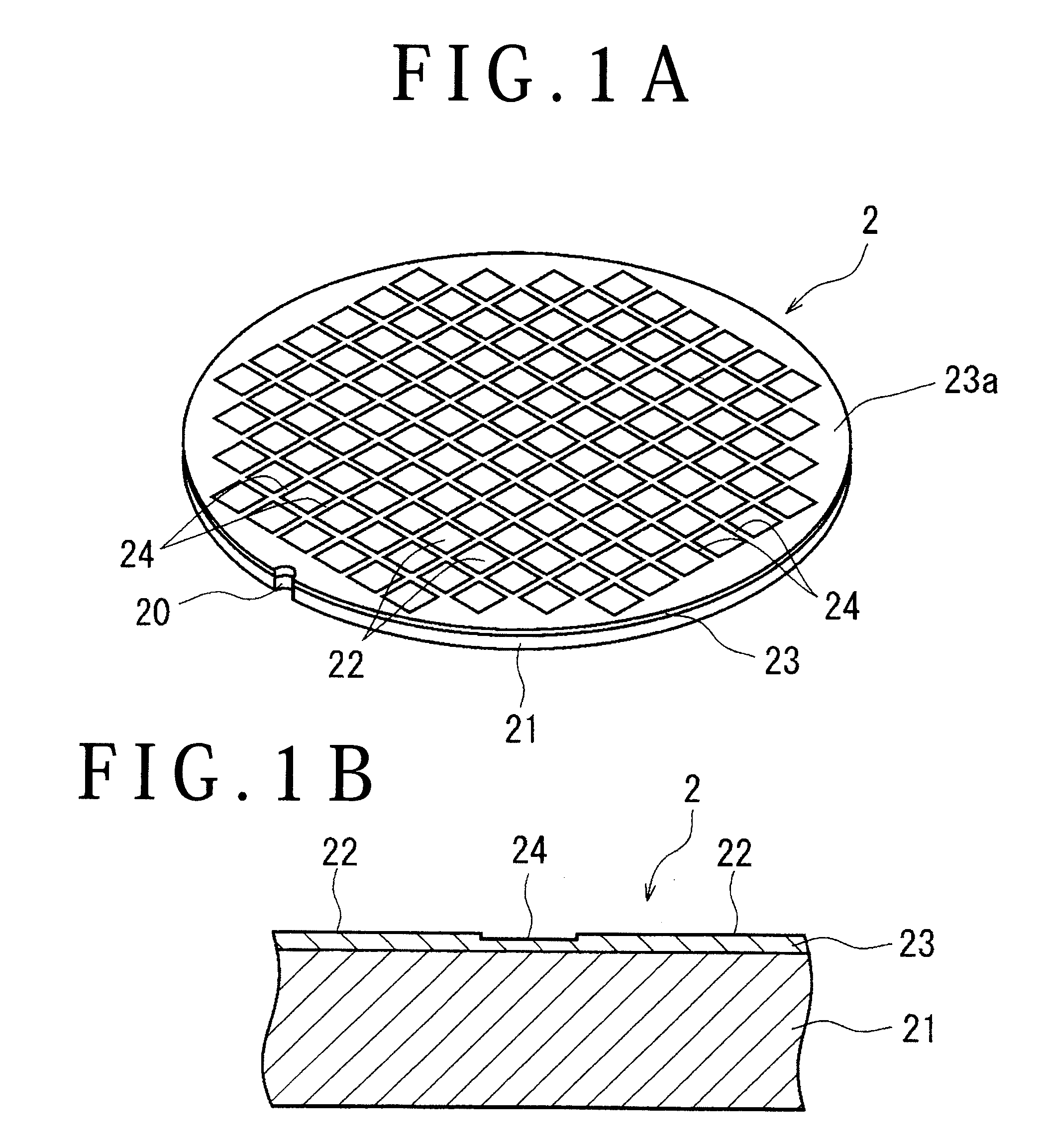
[0028]Preferred embodiments of an optical device manufacturing method according to the present invention will hereinafter be described in detail with reference to the accompanying drawings. An optical device wafer 2 illustrated in FIGS. 1A and 1B is such that an optical device layer 23 forming a plurality of optical devices 22 made of gallium nitride (GaN) or the like is formed on the front surface of a substrate 21 made of sapphire. Lattice-like streets 24 are formed on the front surface 23a of the optical device layer 23 so as to section the optical devices 22. The optical device wafer 2 is formed at an outer circumferential portion with a notch 20 indicating the crystal orientation of the sapphire substrate 21.

[0029]A description is below given of a first embodiment of the optical device manufacturing method in which the optical device wafer 2 is divided into the plurality of optical devices 22 sectioned along the streets 24 and a heat sink is joined to each of the optical device...


PUM

PropertyMeasurementUnit
thicknessaaaaaaaaaa
thicknessaaaaaaaaaa
depthaaaaaaaaaa

Abstract

An optical device manufacturing method including the steps of: forming a groove with a depth corresponding to a finish thickness of the heat sink in a heat sink material at a position corresponding to an associated one of the streets sectioning the plurality of optical devices; joining the optical device layer of the optical device wafer to the heat sink material via a joining metal layer; cutting and dividing the optical device wafer along the streets into individual optical devices; sticking a protection member to the rear surface of the substrate of the optical device wafer; and grinding the rear surface of the heat sink material to expose the grooves to the rear surface to thereby divide the heat sink material into heat sinks corresponding to associated individual optical devices.

Description

BACKGROUND OF THE INVENTION[0001]1. Field of the Invention[0002]The present invention relates to an optical device manufacturing method of dividing an optical device wafer into a plurality of optical devices sectioned along streets and joining a heat sink to each of the optical devices, the optical device wafer being formed with the optical devices in an optical device layer lying on the front surface of a substrate.[0003]2. Description of the Related Art[0004]In the optical device manufacturing step, a plurality of optical devices are formed in an optical device layer made of a gallium nitride-based compound semiconductor or the like on the front surface of a sapphire substrate, a silicon carbide substrate or the like. An optical device wafer formed with the optical devices in the optical device layer as mentioned above is divided into the individual optical devices sectioned along streets for manufacture.[0005]As a method of dividing an optical device wafer along streets, a method...

Claims


Application Information

Patent Timeline
17 Sep 2009
Publication
US20090233419A1
IPC
H01L21/302; B23K26/38; B23K26/40; C30B29/38; C30B33/00; H01L21/301; H01L21/304; H01L33/32; H01L33/48
CPC
H01L33/0079; H01L33/0095; H01S5/0201; H01L2933/0075; H01L33/64; H01L33/0093
Inventors
ARAI, KAZUHISA