Ceramic heater

a ceramic heater and heater plate technology, applied in the direction of coatings, metallic material coating processes, chemical vapor deposition coatings, etc., can solve the problems of deteriorating the quality of the film to be formed on the substrate, non-uniform temperature distribution in the substrate, and forming a dent in the region, so as to improve the temperature uniformity, deteriorating the temperature uniformity, and increasing the amount of purge gas ejected from the vicinity of the purge hole 24

Active Publication Date: 2009-09-24
NGK INSULATORS LTD
View PDF8 Cites 58 Cited by
  • Summary
  • Abstract
  • Description
  • Claims
  • Application Information

AI Technical Summary

Benefits of technology

[0077]By setting the dimension of each component as described below, a purge gas accumulated in a space inside the annularly-formed purge groove 20 is ejected toward the convex portion 12a uniformly through the gap between the substrate 50 and the mounting surface 12b of the first base 12 (particularly, the surface of the second region 23). Thereby, the effects of the invention of the present application are exerted significantly.
[0078]The width Wt of the purge groove 20 is desirably in a range between 0.5 mm and 4 mm. If the width Wt is less than 0.5 mm, the pressure of a supplied purge gas increases, thus causing the substrate 50 to float. On the other hand, if the width Wt exceeds 4 mm, the substrate 50 above the purge groove 20 is heated insufficiently, which deteriorates the temperature uniformity.
[0079]The depth Tt of the purge groove 20 is desirably in a range between 0.025 mm and 0.25 mm. If the depth Tt is less than 0.025 mm, the pressure of a supplied purge gas increases, which causes the substrate 50 to float and thereby deteriorates the temperature uniformity. On the other hand, if the depth Tt exceeds 0.25 mm, the substrate 50 above the purge groove 20 is heated insufficiently, which deteriorates the temperature uniformity.
[0080]The surface-to-surface distance Tg between the first region 22 and the second region 23 is desirably in a range between 0.01 mm and 0.1 mm. If the surface-to-surface distance Tg is less than 0.01 mm, the surface of the first region 22 is located substantially at the same level as that of the second region 23 as in Comparative Example to be described later. Accordingly, the substrate 50 partially comes into contact with the surface of the second region 23. For this reason, a purge gas cannot uniformly flow toward the outer edge portion of the first base 12 from the back surface side, in the vicinity of the outer edge, of the substrate 50. To put it differently, the flow of the purge gas is partially blocked by the contact portion between the substrate 50 and the surface of the second region 23; thus, a corrosive gas stays in the vicinity of the side wall of the convex portion 12a provided at the outer edge portion of the first base 12. As a result, a part of the surface in a region of the second region 23 is corroded, the region formed between the outer edge of the substrate 50 and the convex portion 12a of the first base 12 by the staying corrosive gas. On the other hand, if the surface-to-surface distance Tg exceeds 0.1 mm, the purge gas is ejected in a non-uniform manner from the gap between the surface of the second region 23 and the back surface, in the vicinity of the outer edge, of the substrate 50; more specifically, the amount of the purge gas ejected from the vicinity of the purge holes 24 is increased. Furthermore, the surface-to-surface distance Tg exceeding 0.1 mm adversely affects the temperature uniformity of the substrate 50.
[0081]The diameter D of the purge hole 24 is desirably in a range between 0.25 mm and 2 mm. If the diameter D is less than 0.25 mm, a purge gas cannot flow at a sufficient flow rate, thus resulting in insufficient removal (purge) of a corrosive gas. On the other hand, if the diameter D exceeds 2 mm, a purge gas cools the outer periphery of the substrate 50, which deteriorates the temperature uniformity of the outer periphery thereof.
[0082]The PCD of the purge holes 24 is desirably in a range between 280 mm and 299 mm. If the PCD is less than 280 mm, a purge gas is supplied to the vicinity of a central region of the substrate 50, which deteriorates the temperature uniformity. On the other hand, if the PCD exceeds 299 mm, the gap portion sandwiched between the back surface of the substrate 50 and the surface of the second region 23 is narrowed. This makes it difficult for a purge gas to flow toward the convex portion 12a provided at the outer edge portion of the upper surface of the first base 12. This, in turn, makes it easier for a corrosive gas to flow from the outer edge of the substrate toward the center thereof. As a result, the corrosive gas goes around the back surface of the substrate 50, thereby corroding the upper surface of the first base 12. Accordingly, the quality of a film to be formed on the substrate 50 is deteriorated.

Problems solved by technology

Particularly, when the upper surface of the plate has a pocket shape, the following problem arises.
For this reason, of the mounting surface, AlN corrosion is significant in a region in the vicinity of the outer edge portion of the substrate, forming a dent in the region.
The corroded dent changes the degree of contact between the substrate and the ceramic heater in the region; such a change in the degree of contact causes the temperature distribution in the substrate to be non-uniform.
As a result, a problem arises that using the ceramic heater for a long period deteriorates the quality of a film to be formed on the substrate.
This causes problems including: decrease in the resistance of the plate to thermal stress; change in the density of plasma generated in the reaction chamber; change in the temperature uniformity due to decrease in the heat capacity of the ceramic heater along with decrease in the thickness of the plate; and the like.
In the semiconductor fabricating process after the CVD process, the fine particles deposited on the back surface of the substrate are separated, which causes particle contamination.

Method used


Image

  • Ceramic heater
  • Ceramic heater
  • Ceramic heater

Examples


embodiment

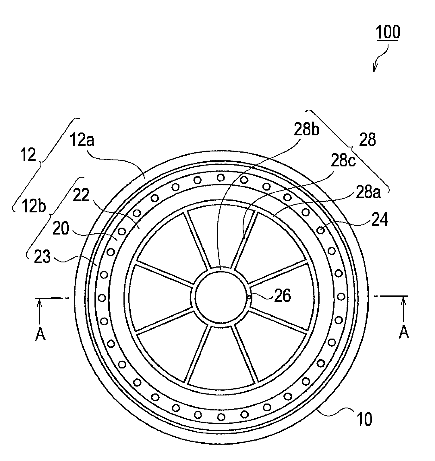
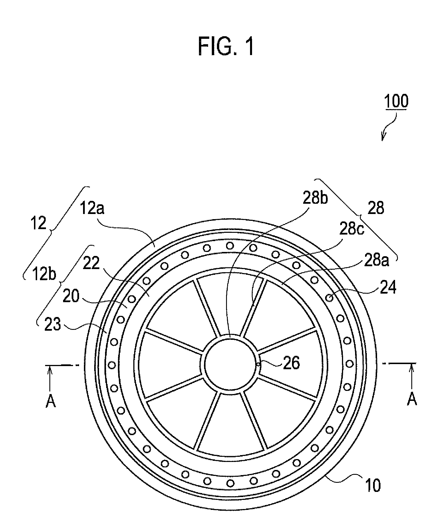
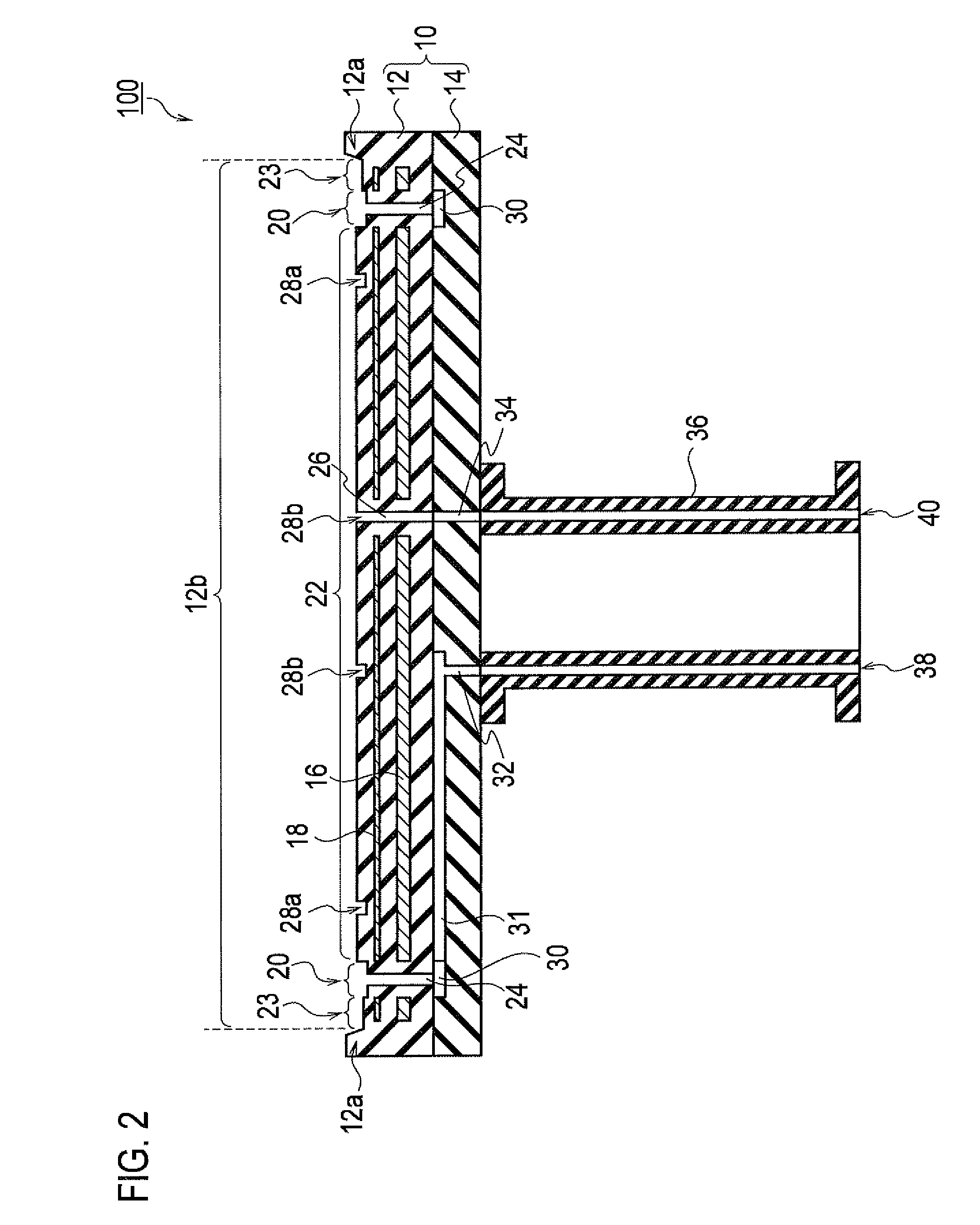
[0045](1) Structure of Ceramic Heater

[0046]Hereinafter, a structure of the ceramic heater according to the embodiment of the present invention will be described with reference to the drawings.

[0047](1.1) Schematic Structure of Ceramic Heater

[0048]FIG. 1 is a plan view showing one example of a ceramic heater 100 according to the embodiment the present invention. FIG. 2 is a schematic diagram showing the cross-section of the ceramic heater 100 shown in FIG. 1 taken along the line A-A. As shown in FIGS. 1 and 2, the ceramic heater 100 includes: a plate 10 on which a substrate (unillustrated) is mounted; a shaft 36 configured to support the plate 10; and the like. The plate 10 includes a first base 12 and a second base 14. The upper surface of the second base 14 is bonded to the lower surface of the first base 12. One end of the shaft 36 is bonded to the lower surface of the second base 14. Note that, hereinafter, one end of the shaft 36 refers to one of the end portions of the shaft 36...

modification example 1

[0107]Hereinafter, a ceramic heater 100 according to Modification Example 1 of the embodiment of the present invention will be described.

[0108]In the above-described embodiment of the present invention, the description has been given of the case where the first base 12 has the vacuum chuck groove 28 configured to vacuum-adsorb a substrate onto the mounting surface 12b. However, the present invention is not limited to this. For example, a space larger than the vacuum chuck groove 28 may be formed between the substrate and the mounting surface 12b as a space to be evacuated.

[0109]The structure of the ceramic heater 100 according to Modification Example 1 will be described with reference to FIGS. 6 and 7. FIG. 6 is a plan view showing the ceramic heater 100 according to Modification Example 1. FIG. 7 is a schematic diagram showing the cross-section of the ceramic heater 100 shown in FIG. 6 taken along the line B-B. Hereinafter, description will be mainly given of the difference between...

modification example 2

[0117]Hereinafter, a ceramic heater 100 according to Modification Example 2 of the embodiment of the present invention will be described.

[0118]In the above-described embodiment of the present invention, the description has been given of the case where the vacuum chuck is used to hold a substrate on the mounting surface 12b. However, the present invention is not limited to this. For example, an electrostatic chuck may be used to hold a substrate on the mounting surface 12b.

[0119]The structure of the ceramic heater 100 according to Modification Example 2 will be described with reference to FIGS. 8 and 9. FIG. 8 is a plan view of the ceramic heater 100 according to Modification Example 2. FIG. 9 is a schematic diagram showing the cross-section of the ceramic heater 100 shown in FIG. 8 taken along the line C-C. Hereinafter, description will be mainly given of the difference between the above-described embodiment and Modification Example 2.

[0120]As shown in FIGS. 8 and 9, the first regi...


PUM

PropertyMeasurementUnit
diameteraaaaaaaaaa
widthaaaaaaaaaa
widthaaaaaaaaaa

Abstract

A ceramic heater for a semiconductor substrate process includes a plate and a shaft. The plate includes a first base and a second base bonded to the first base. Defined on a mounting surface of the first base are: a first region having a surface contacting with a mounted substrate; a purge groove provided in the portion covered with the substrate and surrounds the first region; and a second region having a surface surrounding the purge groove. The first base has: an adsorber configured to adsorb the mounted substrate onto the surface of the first region; and multiple purge holes each penetrating from the bottom surface of the purge groove to the lower surface of the first base. The purge groove is supplied with a purge gas through the multiple purge holes. The surface of the second region is located lower than that of the first region.

Description

CROSS-REFERENCE TO RELATED APPLICATIONS[0001]This application is based upon and claims the benefit of priority from prior Japanese Patent Application P2008-74478 filed on Mar. 21, 2008, and Japanese Patent Application P2009-68611 filed on Mar. 19, 2009; the entire contents of which are incorporated by reference herein.BACKGROUND OF THE INVENTION[0002]1. Field of the Invention[0003]The present invention relates to a ceramic heater used for an electronic-device manufacturing apparatus.[0004]2. Description of the Related Art[0005]In the process of manufacturing electronic devices such as semiconductor devices and liquid crystal devices, high-temperature processes such as chemical vapor deposition (CVD) and surface modification are employed. For example, in CVD, a semiconductor substrate to be processed is mounted on a ceramic heater provided in a reaction chamber of a CVD apparatus. Films such as a semiconductor film and an insulating film are formed on the substrate which is heated by...

Claims


Application Information

Patent Timeline
Patent Type & Authority Applications(United States)
IPC IPC(8): C23C16/54
CPCC23C16/45521C23C16/4586H01L21/68757H01L21/6875H01L21/67103
Inventor KATAIGI, TAKASHIAKATSUKA, YUJI
Owner NGK INSULATORS LTD
Why Eureka
Try Eureka