

Process variation compensated multi-chip memory package
- Summary
- Abstract
- Description
- Claims
- Application Information
AI Technical Summary
Benefits of technology
Problems solved by technology
Method used
Image

Examples
Embodiment Construction
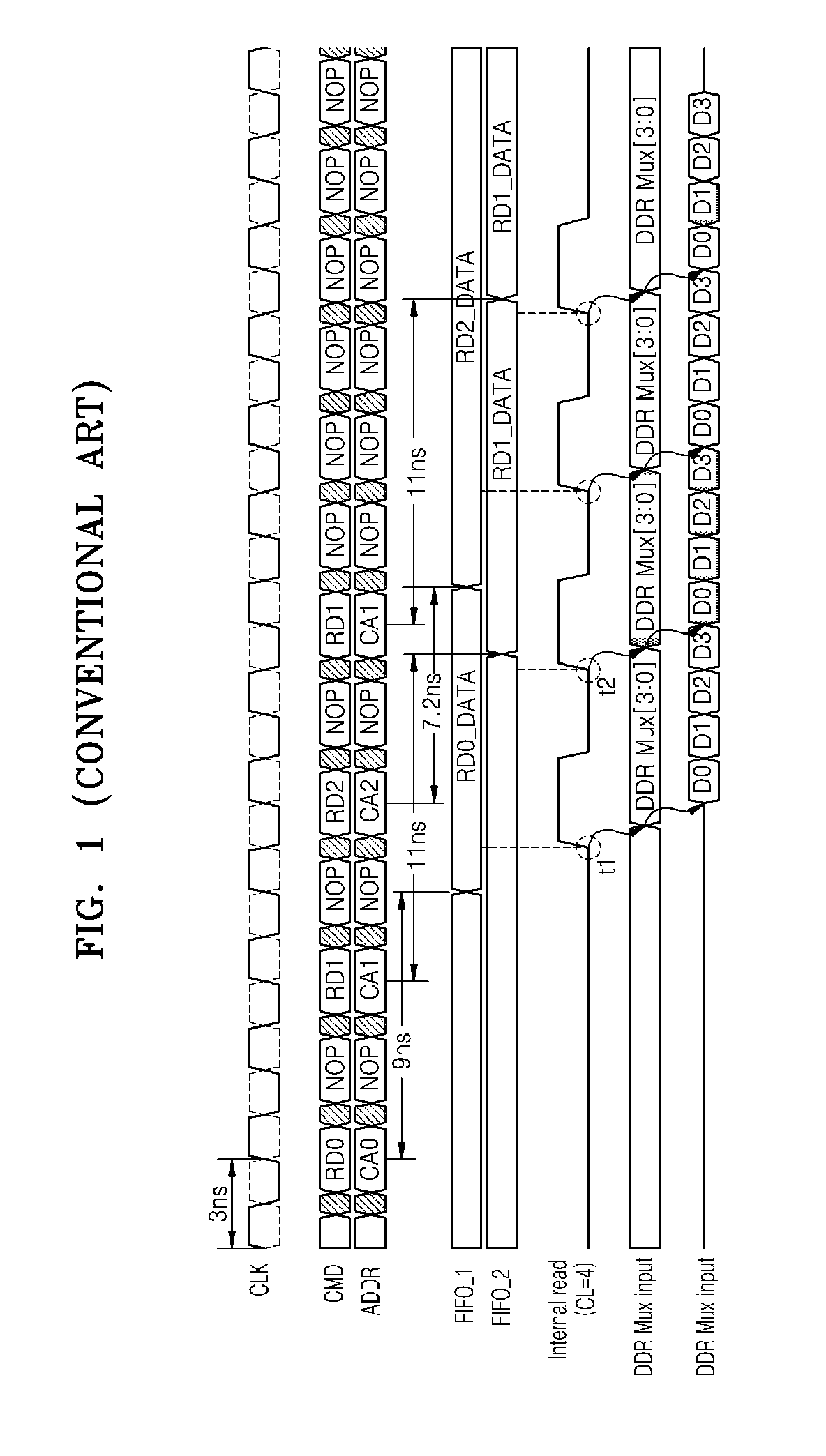
[0019]The difficulties noted above in relation to conventional multi-chip package memories and related process variations are further illustrated by way of background information in relation to FIG. 1. FIG. 1 is a signal and data waveform diagram characterizing a read operation executed in accordance with a technique associated with a conventional multi-chip package memory.
[0020]Within FIG. 1, a first read command RD0 is applied to a first memory chip within a stacked plurality of memory chips, a second read command RD1 is applied to a second memory chip, and a third read command RD2 is applied to a third memory chip. Taking into account all relevant process variations, the first memory chip outputs read data in 9 ns. That is, a first time interval between receipt (input) of the first read command RD0 and provision (output) of the corresponding first read data RD0_DATA by an associated first FIFO (First-In-First-Out Buffer) FIFO_1 is 9 ns. In similar manner, process variation associ...
PUM
 Abstract
Description
Claims
Application Information