
Liquid crystal display device, method for manufacturing the same, and electronic apparatus

a liquid crystal display and liquid crystal technology, applied in the direction of thin material processing, instruments, coatings, etc., can solve the problems of low productive efficiency as compared with conventional coating process, large initial investment cost, and difficult to say that conventional coating process has advantages in productive efficiency as well as costs, so as to prevent display failure, reduce costs, and good contrast characteristics

Inactive Publication Date: 2009-09-24
SEIKO EPSON CORP
View PDF9 Cites 7 Cited by
  • Summary
  • Abstract
  • Description
  • Claims
  • Application Information

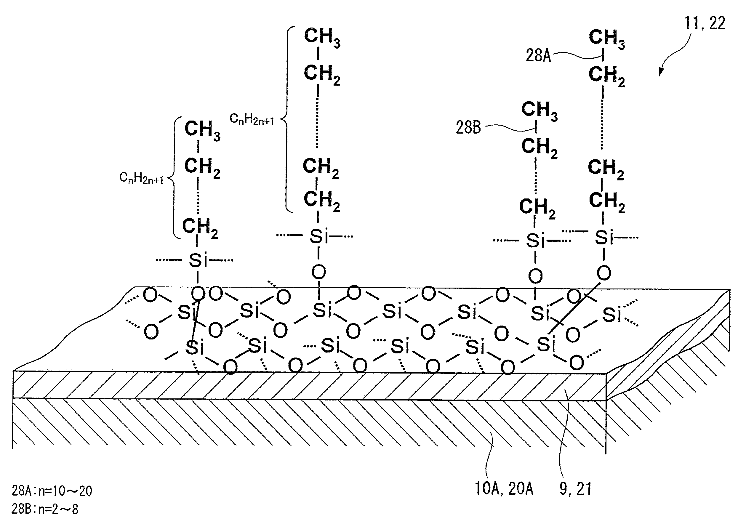
AI Technical Summary

Benefits of technology

[0009]An advantage of the invention is to provide a liquid crystal display device having a good contrast characteristic while preventing display failures such as disclination lines and enabling costs to be reduced, a method for manufacturing the liquid crystal display device, and an electronic apparatus using the device.
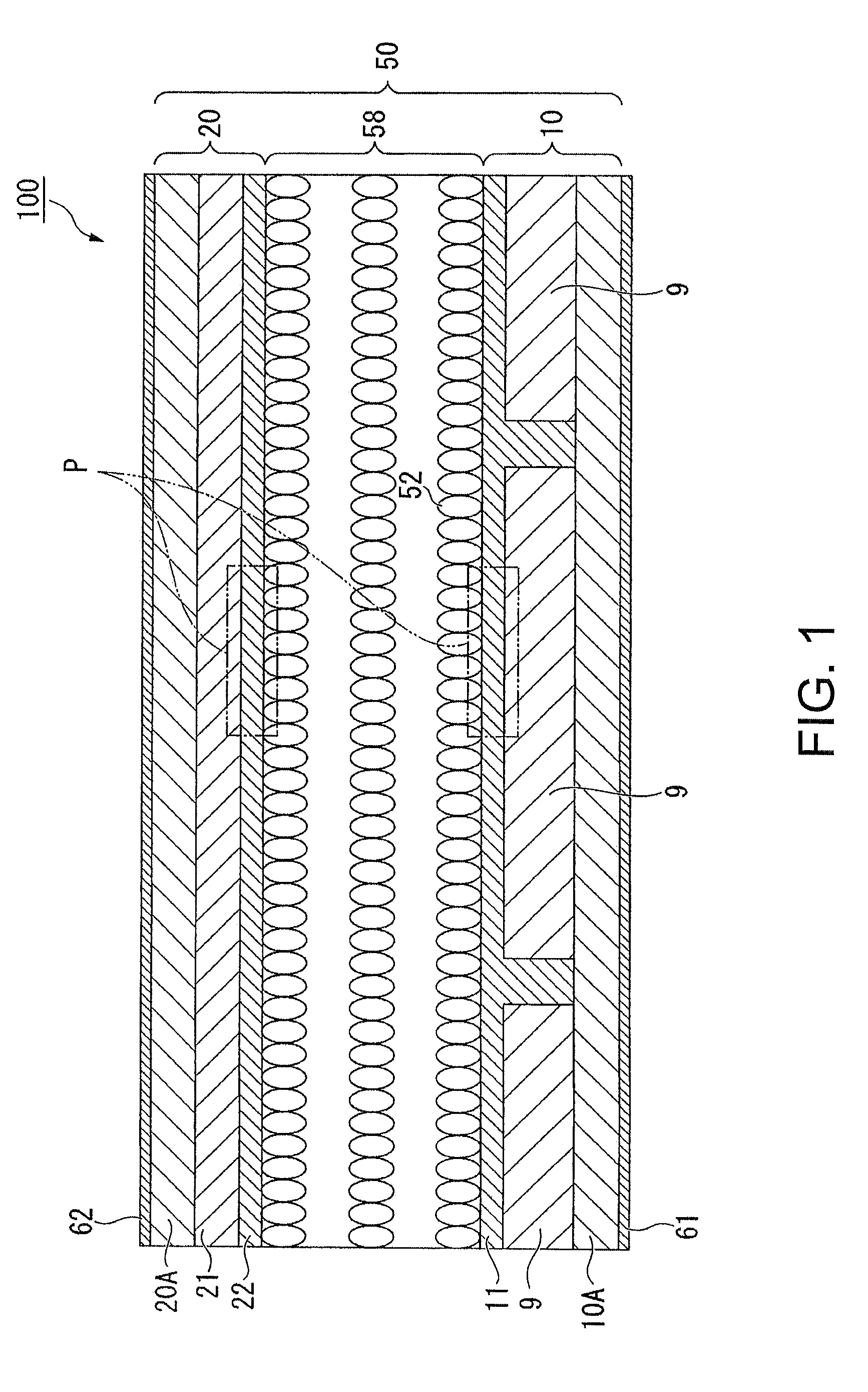
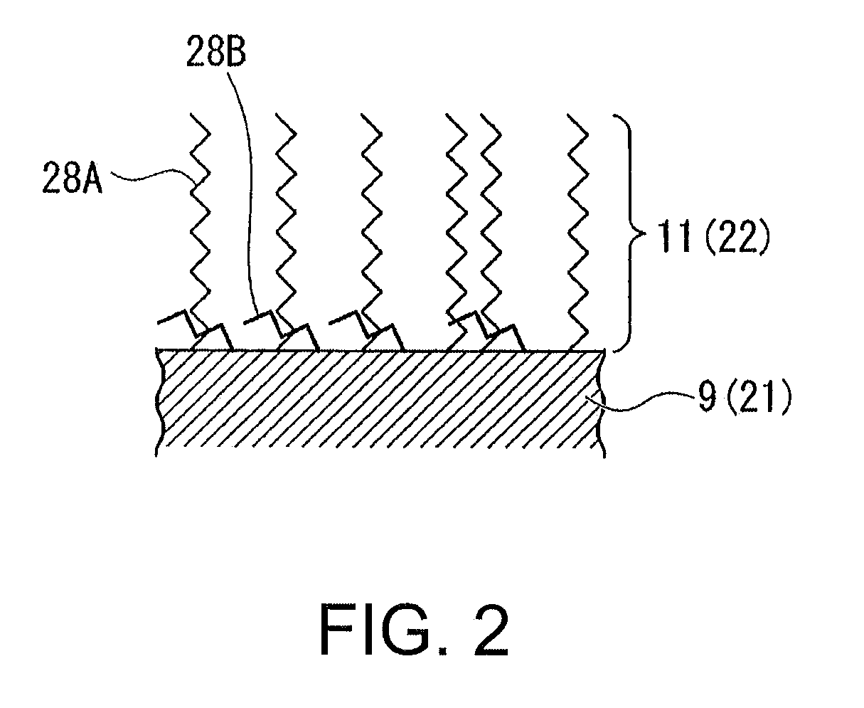
[0010]According to a first aspect of the invention, a liquid crystal display device includes a pair of substrates, and a liquid crystal layer that is vertically aligned in an initial state and sandwiched between the pair of the substrates. In the device, an alignment layer existing on an uppermost surface of at least one of the substrates is composed of alkyl chains having a different chain length each other, and an alkyl chain having a shortest chain length in the alkyl chains is tilted to the uppermost surface of the at least one of the substrates.
[0011]The device has a pair of substrates. The alignment layer on at least one of the substrates has alkyl chains having a different alkyl chain length each other, i.e., alkyl chains having the number of carbon atoms different each other. The alkyl chain having the number of carbon atoms (chain length) smallest in the alkyl chains is tilted to the substrate surface. As a result, the pretilt is given to the alignment layer. This alignment layer makes it possible that the liquid crystal molecules are vertically aligned with the alkyl chain having the long chain length when applying no voltage, while the liquid crystal molecules are aligned in a one-axis direction with the alkyl chain that is tilted to the substrate surface and has the shortest chain length when applying a voltage.
[0012]According to a second aspect of the invention, a method for manufacturing a liquid crystal display device that includes a pair of substrates and a liquid crystal layer that is vertically aligned at an initial state and sandwiched between the pair of the substrates, includes: (a) reacting at least two kinds or more of silane coupling agents having a different alkyl chain length each other with a surface of at least one of the pair of the substrates, the surface facing the liquid crystal layer; and (b) tilting an alkyl chain having a shortest chain length of the different alkyl chain lengths to the surface of the at least one of the substrates.
[0013]The device has a pair of substrates. The alignment layer provided on at least one of the substrates has alkyl chains having a different alkyl chain length each other. The alkyl chain having the shortest chain length in the alkyl chains is tilted to the substrate surface. As a result, the pretilt is given to the alignment layer. This alignment layer makes it possible that the liquid crystal molecules are practically vertically aligned with the alkyl chain having the longest chain length when applying no voltage while the liquid crystal molecules are aligned in a one-axis direction with the alkyl chain that is tilted to the substrate surface and has the shortest chain length when applying a voltage.
[0014]In the step (a), the silane coupling agents come into contact with a surface on which a film may be formed of the at least one of the substrates in an order from a silane coupling agent containing an alkyl group having a longest chain length of the silane coupling agents.

Problems solved by technology

Mass producing the liquid crystal display devices, however, needs expensive equipments such as high vacuum deposition system, causing large initial investment costs and also low productive efficiency as compared with conventional coating processes.
These methods are based on the steps of forming an inorganic alignment layer such as SiO2 and surface treating the alignment layer, making it hard to say they have advantages in productive efficiency as well as costs.
The method disclosed in the fourth example, however, does not fully one-axis align liquid crystal molecules when applying a voltage.

Method used


Image

  • Liquid crystal display device, method for manufacturing the same, and electronic apparatus
  • Liquid crystal display device, method for manufacturing the same, and electronic apparatus
  • Liquid crystal display device, method for manufacturing the same, and electronic apparatus

Examples


example 1

[0084]A 1% by weight solution of octadecyltriethoxysilane in methanol solution was prepared. The circuit substrate 10 and the counter substrate 20 were immersed in the solution for 30 minutes, and then taken out. The substrates were cleaned with dekalin, and then heated at 120 degrees centigrade for 1 hour in a heated oven (a long-chain alkyl chain process). Then, the circuit substrate 10 and the counter substrate 20 were immersed in a 1% by weight solution of butyltrimethoxysilane in methanol for 30 minutes. Subsequently, the cleaning and drying were conducted in the same manner as described above. This was a short-chain alkyl chain process.

[0085]The surfaces of the circuit substrate 10 and the counter substrates 20 were subjected to the rubbing process with a typical rubbing process device in such a manner that the set rubbing directions are aligned with a one-axis direction when the substrates are combined. The surfaces face the liquid crystal layer and were surface treated with ...


PUM

PropertyMeasurementUnit
chain lengthaaaaaaaaaa
durabilityaaaaaaaaaa
humidity resistanceaaaaaaaaaa

Abstract

A liquid crystal display device includes a pair of substrates, and a liquid crystal layer that is vertically aligned in an initial state and sandwiched between the pair of the substrates. In the device, an alignment layer existing on an uppermost surface of at least one of the substrates is composed of alkyl chains having a different chain length each other, and an alkyl chain having a shortest chain length in the alkyl chains is tilted to the uppermost surface of the at least one of the substrates.

Description

CROSS-REFERENCE TO RELATED APPLICATION[0001]This application is based on and claims priority from Japanese Patent Application No. 2008-069224, filed on Mar. 18, 2008, the contents of which are incorporated herein by reference.BACKGROUND[0002]1. Technical Field[0003]The present invention relates to a liquid crystal display device, a method for manufacturing the liquid crystal display device, and an electronic apparatus.[0004]2. Related Art[0005]In recent years, a vertical alignment mode has been increasingly employed in a liquid crystal display device for a projector as a liquid crystal alignment mode. For forming a vertically aligned layer, a method has been generally known in which inorganic molecules such as SiO2 and SiO3 are deposited on electrode surfaces by means of high vacuum deposition processes such as an oblique evaporation method. This method is featured in that no rubbing process is required and a pretilt is easily developed that functions to tilt liquid crystal molecule...

Claims


Application Information

Patent Timeline
Patent Type & Authority Applications(United States)
IPC IPC(8): C09K19/54B05D5/06
CPCG02F1/133719Y10T428/1005G02F2001/133742C09K2323/02G02F1/133742
Inventor NAGAE, NOBUKAZU
Owner SEIKO EPSON CORP
Learn More