Method and Apparatus for Measuring Dimension of Circuit Patterm Formed on Substrate by Using Scanning Electron Microscope

a technology of scanning electron microscope and circuit patterm, which is applied in the direction of material analysis using wave/particle radiation, instruments, nuclear engineering, etc., can solve the problems of not considering sharing the imaging/measurement data obtained from a plurality of devices, getting unrealistic to create the recipe manually, and increasing the number of eps required to be evaluated, so as to reduce the correction of the recipe and improve the imaging accuracy

Active Publication Date: 2009-10-01
HITACHI HIGH-TECH CORP
View PDF2 Cites 29 Cited by
  • Summary
  • Abstract
  • Description
  • Claims
  • Application Information

AI Technical Summary

Benefits of technology

[0011]The present invention relates to an SEM device provided with an automatic creation function for the imaging/measurement recipe and a method therefor, and is in particular for providing a recipe creation method expected to so

Problems solved by technology

Further, as the pattern becomes miniaturized and complicated, the number of EP required to be evaluated increases explosively, and it is getting unrealistic to create the recipe

Method used


Image

  • Method and Apparatus for Measuring Dimension of Circuit Patterm Formed on Substrate by Using Scanning Electron Microscope
  • Method and Apparatus for Measuring Dimension of Circuit Patterm Formed on Substrate by Using Scanning Electron Microscope
  • Method and Apparatus for Measuring Dimension of Circuit Patterm Formed on Substrate by Using Scanning Electron Microscope

Examples


Embodiment Construction

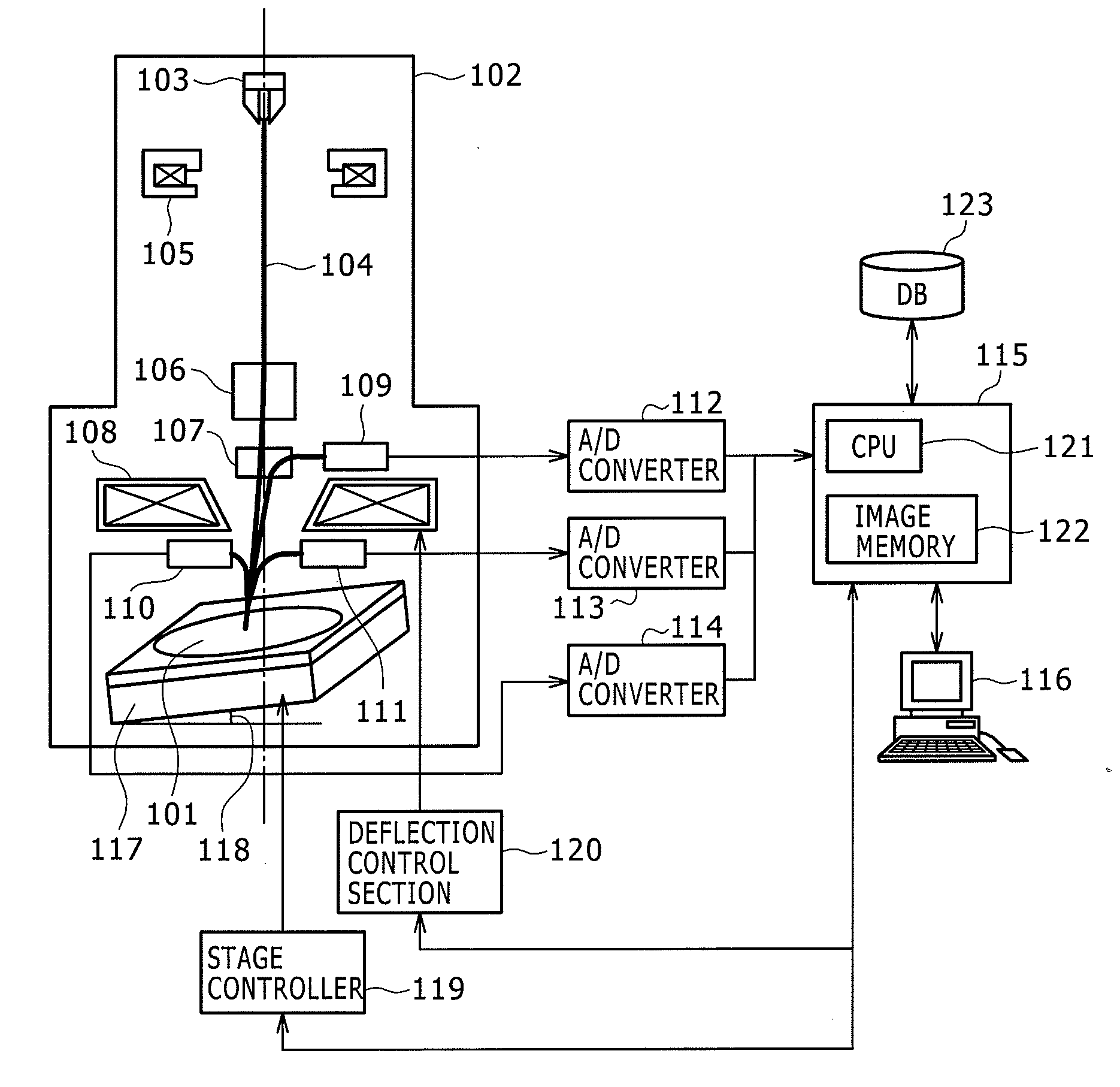
[0062]The present invention relates to an SEM device provided with a function of automatically creating the recipe with the following means, and executing automatic imaging / measurement using the recipe, and a method therefor.

[0063](1) According to a feature of the present invention, coordinate data of EPs and design data of circuit patterns including the EPs are used as an input, creation of the dimension measurement cursor for measuring the patterns existing in the EPs and selection or setting of the dimension measurement method are performed automatically based on the EP coordinate data and the design data. The dimension measurement cursor and the dimension measurement method are stored as a recipe. By performing the processing based on the resign data, there is no need for taking an SEM image when creating the recipe, and therefore, the operation can be carried out online, which leads to an improvement of the operation rate of the apparatus. As the coordinates of the EPs, there a...


PUM


Abstract

In the dimension measurement of a circuit pattern using a scanning electron microscope (SEM), in order to make it possible to automatically image desired evaluation points (EPs) on a sample, and automatically measure the circuit pattern formed at the evaluation points, according to the present invention, in the dimension measurement of a circuit pattern using a scanning electron microscope (SEM), it is arranged that coordinate data of the EP and design data of the circuit pattern including the EP are used as an input, creation of a dimension measurement cursor for measuring the pattern existing in the EP and selection or setting of the dimension measurement method are automatically performed based on the EP coordinate data and the design data to automatically create a recipe, and automatic imaging/measurement is performed using the recipe.

Description

BACKGROUND OF THE INVENTION [0001]The present invention relates to a scanning electron microscope (SEM) capable of imaging a desired evaluation point on a sample and automatically measuring a desired dimension of a circuit pattern formed at the evaluation point, and to a measuring method therefor. Specifically, the present invention relates to an SEM device provided with an automatic recipe creating function of obtaining an SEM image of the desired evaluation point and automatically determining a recipe making it possible to perform a desired measurement (e.g., a measurement of wiring width of the line pattern or a measurement of a gap between the line patterns) at the evaluation point based on the design data of the circuit pattern without using a real wafer, and to a measuring method therefor. In the recipe, there are designated an imaging method of the SEM image of the evaluation point, a position and a shape of a dimension measurement cursor for measuring the dimension in the de...

Claims


Application Information

Patent Timeline
IPC IPC(8): G01N23/00G01B15/00
CPCG01N23/2251G01B15/00
Inventor MIYAMOTO, ATSUSHINISHIURA, TOMOFUMI
Owner HITACHI HIGH-TECH CORP
Why Eureka
Try Eureka