Self-aligned complementary ldmos

a complementary, self-aligning technology, applied in the direction of semiconductor devices, electrical equipment, transistors, etc., can solve the problem of increasing rdson

Active Publication Date: 2009-10-01
SEMICON COMPONENTS IND LLC
View PDF1 Cites 9 Cited by
  • Summary
  • Abstract
  • Description
  • Claims
  • Application Information

AI Technical Summary

Problems solved by technology

Such a drift region, however, increases the Rdson, which in conventional devices is proportional to the pitch between the drain and the source.

Method used


Image

  • Self-aligned complementary ldmos
  • Self-aligned complementary ldmos
  • Self-aligned complementary ldmos

Examples


Embodiment Construction

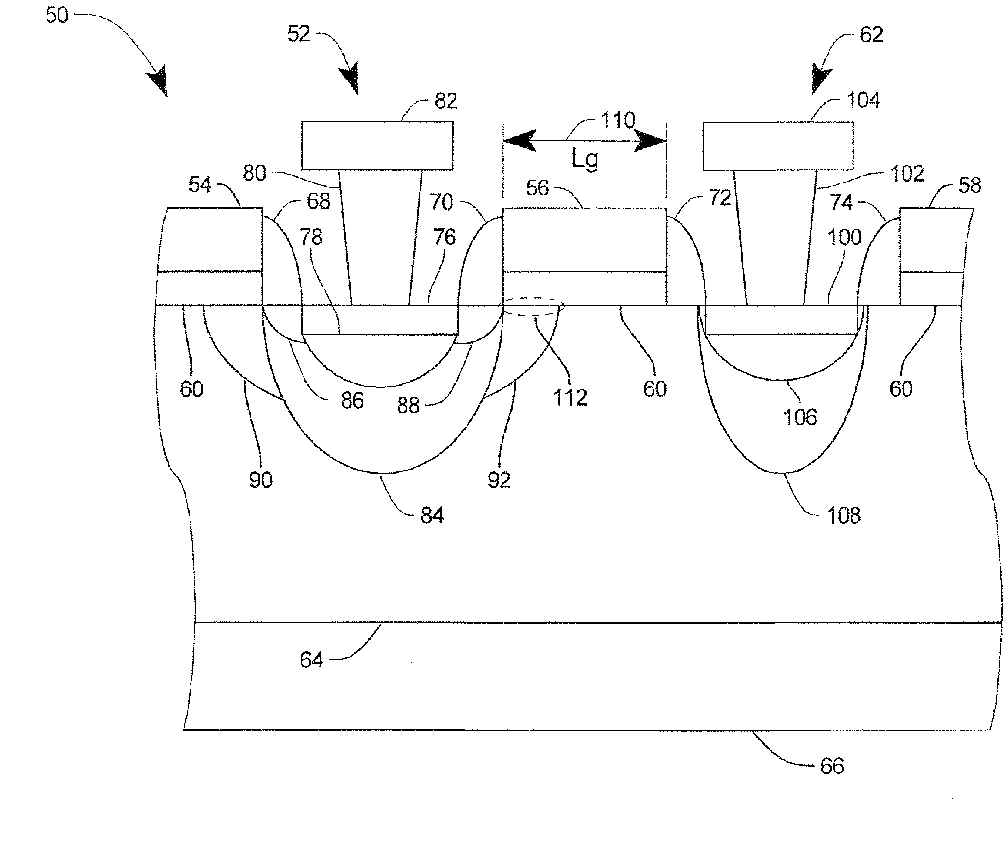
[0047]Referring to FIG. 1, there is shown an n-type embodiment 50 of a fully self-aligned complementary LDMOS device according to one embodiment of the present invention. As shown in FIG. 1 the LDMOS device 50 is a multiple gate device. The LNDMOS 50 includes a source 52, three gates 54, 56, and 58 each having a thick gate oxide 60, and a drain 62. The gate 56 is between the source 52 and the drain 62, while the gate 54 is on the opposite side of the source 52, and the gate 58 is on the opposite side of the drain 62. The source 52 and drain 62 are formed in a high voltage HV NWELL 64. Under the HV NWELL 64 may be another layer 66 which may be an N buried layer or an N isolation layer depending on the use of the LDMOS 50, such as whether the LDMOS 50 is used in a CMOS device or if the LDMOS 50 is subjected to relatively high voltages compared to lower voltage devices in an integrated circuit.

[0048]As shown in FIG. 1 the gate 54 has a right sidewall oxide 68, the gate 56 has a left (o...


PUM


Abstract

The invention includes a laterally double-diffused metal-oxide semiconductor (LDMOS) having a reduced size, a high breakdown voltage, and a low on-state resistance. This is achieved by providing a thick gate oxide on the drain side of the device, which reduces electric field crowding in the off-state to reduce the breakdown voltage and forms an accumulation layer in the drift region to reduce the device resistance in the on-state. A version of the device includes a low voltage version with a thin gate oxide on the source side of the device and a high voltage version of the device includes a thick gate oxide on the source side. The LDMOS may be configured in an LNDMOS having an N type source or an LPDMOS having a P type source. The source of the device is fully aligned under the oxide spacer adjacent the gate to provide a large SOA and to reduce the device leakage.

Description

CROSS REFERENCE TO RELATED APPLICATIONS[0001]This application is a continuation of U.S. patent application Ser. No. 11 / 695,199 filed Apr. 2, 2007, which claims the benefit of U.S. Provisional Application No. 60 / 788,874 filed on Apr. 3, 2006. Both applications are incorporated herein by reference.FIELD OF THE INVENTION[0002]This invention relates to semiconductor devices, and more specifically to LDMOS devices.BACKGROUND OF THE INVENTION[0003]In MOS power devices, such as a lateral double-diffusion metal-oxide semiconductor (LDMOS) device, there is generally a tradeoff between three factors: breakdown voltage (BVdss), on-state resistance (Rdson), and safe operating area (SOA), wherein BVdss and Rdson have a conflicting relationship (e.g., an increase in BVdss results in a higher Rdson), BVdss and SOA aid each other (e.g., an increase in BVdss results in a larger SOA), and Rdson and SOA may have a conflicting or aiding relationship. The BVdss may be increased by spacing the drain regi...

Claims


Application Information

Patent Timeline
Patent Type & Authority Applications(United States)
IPC IPC(8): H01L27/06H01L21/336H01L29/78
CPCH01L21/823807H01L21/823814H01L21/823857H01L27/092H01L29/0869H01L29/66689H01L29/1083H01L29/1087H01L29/42364H01L29/42368H01L29/456H01L29/0878H01L29/7816
Inventor CAI, JUN
Owner SEMICON COMPONENTS IND LLC
Why Eureka
Try Eureka