Pixel and organic light emitting display device including the same

Active Publication Date: 2009-10-01
SAMSUNG DISPLAY CO LTD
View PDF3 Cites 31 Cited by
  • Summary
  • Abstract
  • Description
  • Claims
  • Application Information

AI Technical Summary

Benefits of technology

[0019]An aspects of embodiments of the present invention are directed toward an organic light emitting display device capabl

Problems solved by technology

However, the active matrix type organic light emitting display device has a disadvantage in that its picture quality becomes non-uniform as a result of brightness differences between pixels generated due to threshold voltage variation of driving transistors.
However, in the case of compensating for the threshold voltage

Method used


Image

  • Pixel and organic light emitting display device including the same
  • Pixel and organic light emitting display device including the same
  • Pixel and organic light emitting display device including the same

Examples


Example

[0040]In the following detailed description, only certain exemplary embodiments of the present invention have been shown and described, simply by way of illustration. As those skilled in the art would realize, the described embodiments may be modified in various different ways, all without departing from the spirit or scope of the present invention. Accordingly, the drawings and description are to be regarded as illustrative in nature and not restrictive. Like reference numerals designate like elements throughout the specification. Also, when a first element is described as being coupled to a second element, the first element may be directly coupled to the second element, or may be indirectly coupled to the second element via a third element. Further, some of the elements that are not essential to the complete understanding of the invention are omitted for clarity.

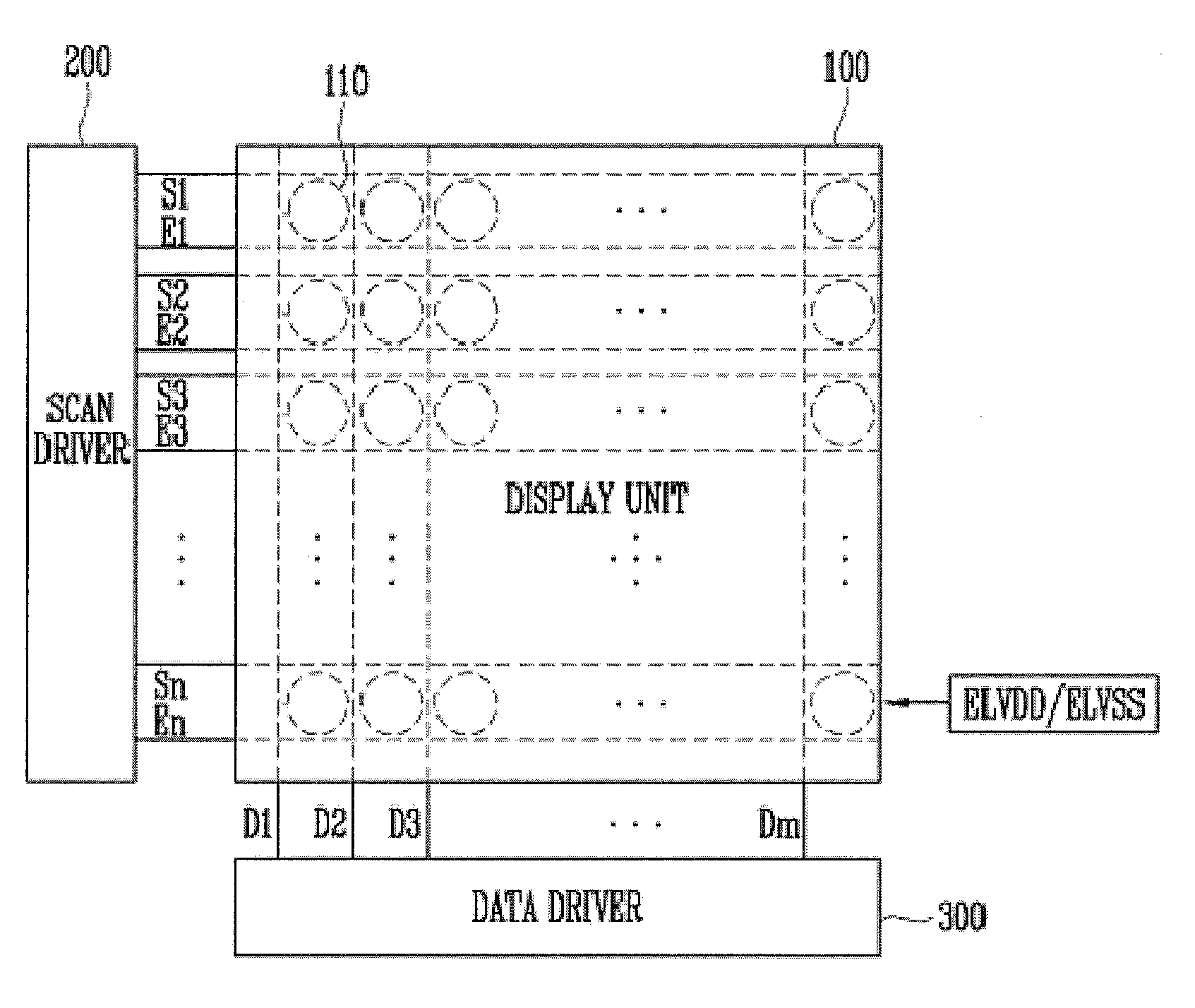
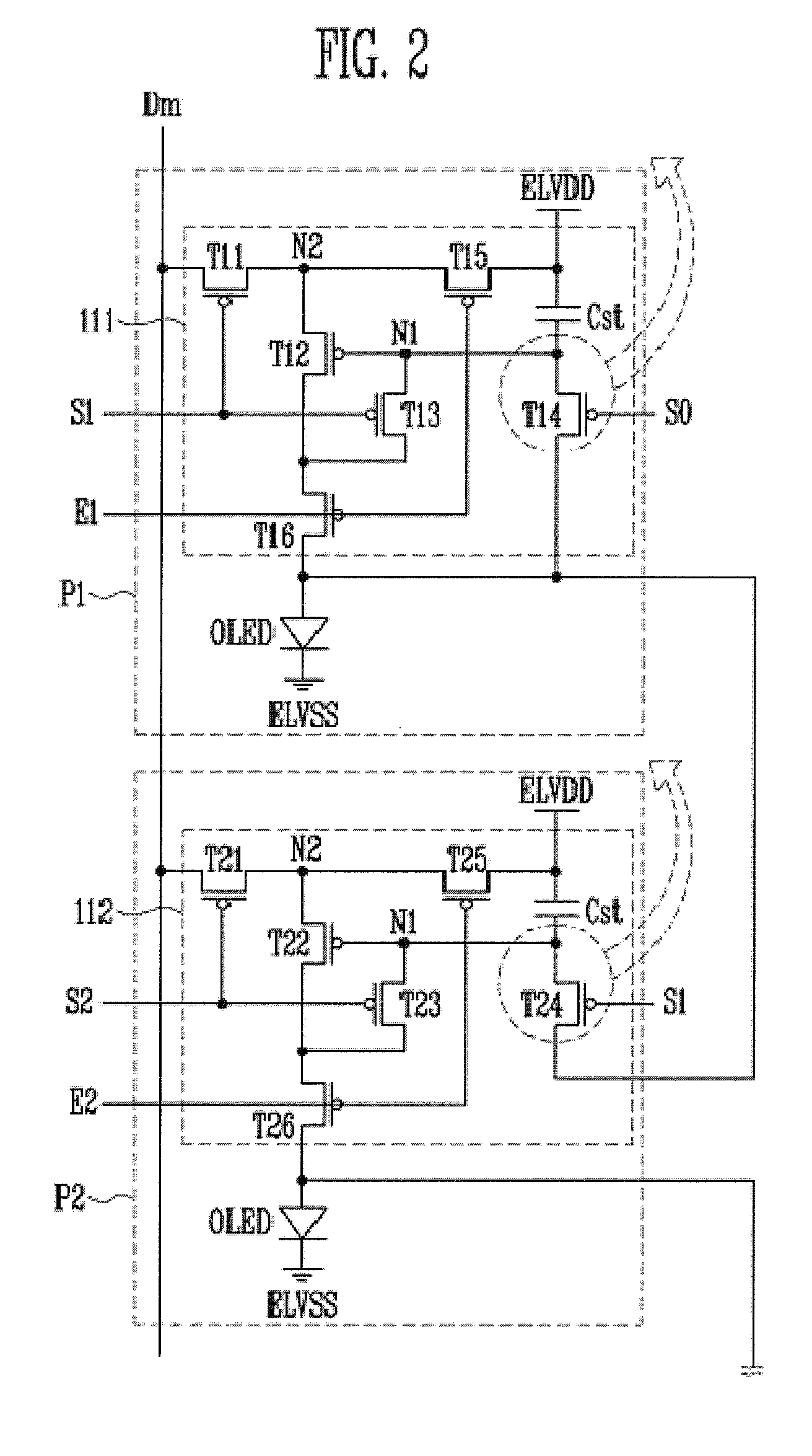
[0041]FIG. 1 is a block diagram showing an organic light emitting display device according to an embodiment of the prese...


PUM


Abstract

An organic light emitting display device including: a plurality of pixels, each of the pixels including an organic light emitting diode (OLED) and a pixel circuit for driving the OLED, the pixel circuit including: a first transistor for transferring a data signal supplied from a data line to a current scan line; a second transistor for controlling an amount of current corresponding to the data signal that flows from a first pixel power supply to the OLED; a third transistor for diode-connecting the second diode according to the current scan signal; a storage capacitor for maintaining a gate voltage of the second transistor in accordance with the data signal; and a fourth transistor for initializing a first node according to a previous scan signal supplied before the current scan signal is supplied, the fourth transistor in a pixel region of a previous row pixel.

Description

CROSS-REFERENCE TO RELATED APPLICATIONS[0001]This application claims priority to and the benefit of Korean Patent Application No. 10-2008-0028884, filed on Mar. 28, 2008, in the Korean Intellectual Property Office, the entire content of which is incorporated herein by reference.BACKGROUND OF THE INVENTION[0002]1. Field of the Invention[0003]The present invention relates to a pixel and an organic light emitting display device including the same.[0004]2. Description of Related Art[0005]Recently, various flat panel display devices having light weight and small volume, as compared to cathode ray tubes, have been developed.[0006]Among the flat panel display devices, organic light emitting display devices have excellent brightness and color purity by displaying images using organic light emitting diodes, which are self-emission devices. Therefore, they are in the spotlight as next generation display devices.[0007]Such organic light emitting display devices can be categorized as passive ma...

Claims


Application Information

Patent Timeline
IPC IPC(8): G09G3/30
CPCG09G3/3233G09G2300/0465G09G2300/0819G09G2320/0233G09G2310/0262G09G2310/061G09G2300/0861G09G3/30G09G3/32G09G3/20H05B33/12
Inventor CHUNG, KYUNG-HOON
Owner SAMSUNG DISPLAY CO LTD
Why Eureka
Try Eureka