Wafer processing method
- Summary
- Abstract
- Description
- Claims
- Application Information
AI Technical Summary
Benefits of technology
Problems solved by technology
Method used
Image
Examples
Embodiment Construction
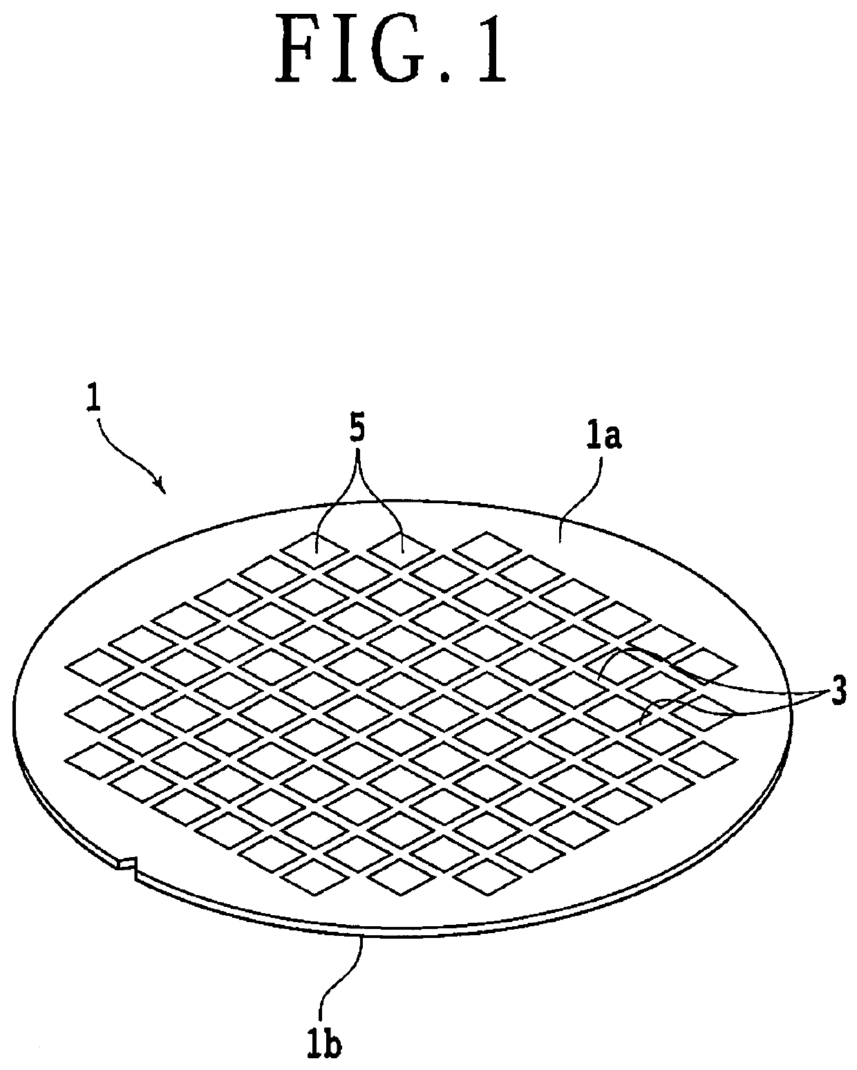
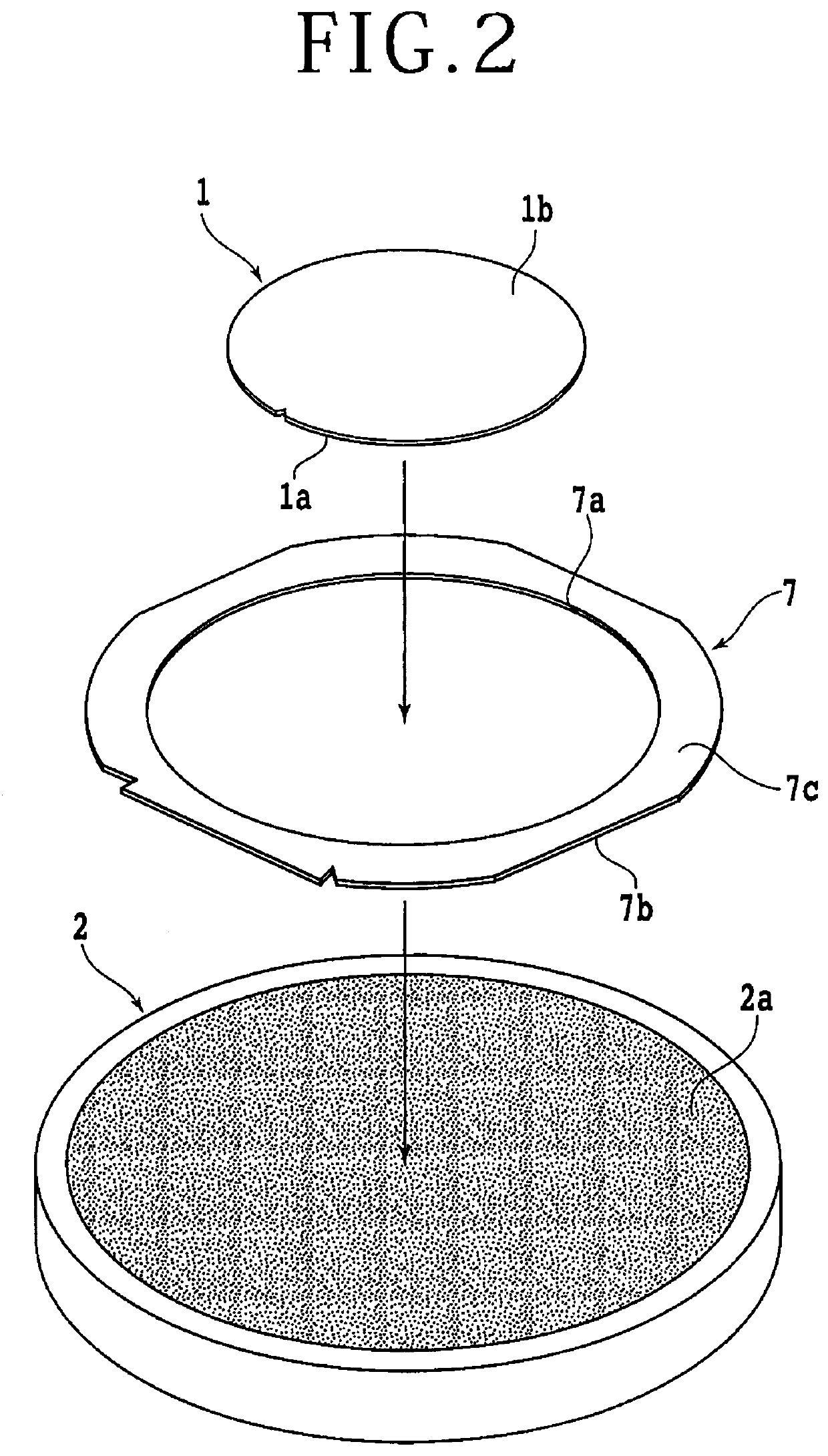
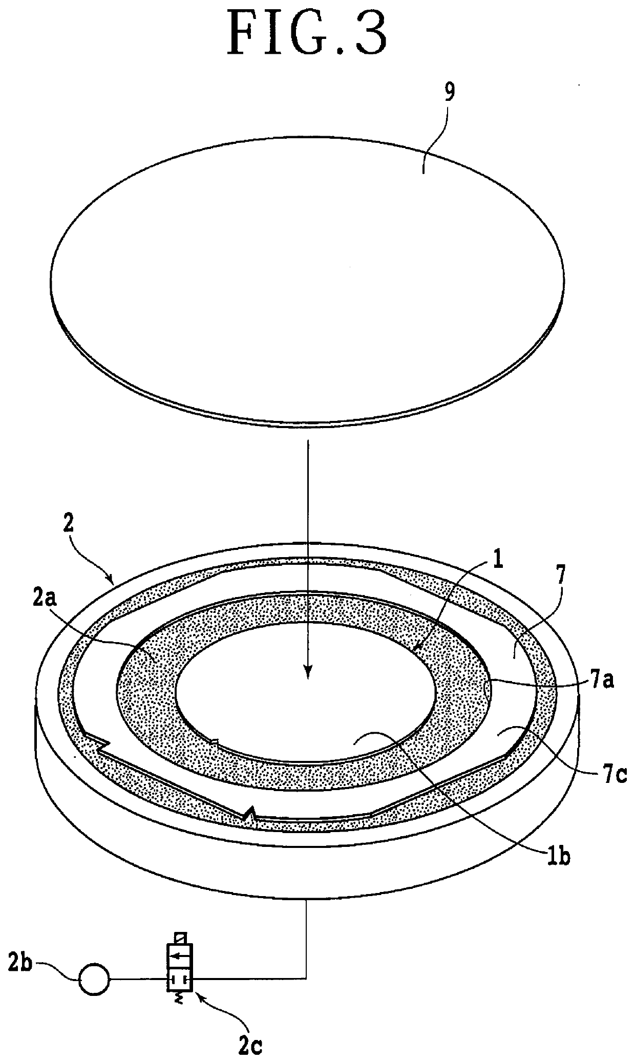
[0030]A preferred embodiment of the present invention will now be described with reference to the attached drawings. There will first be described a wafer to be processed by a processing method according to this preferred embodiment. FIG. 1 is a schematic perspective view of a wafer 1. The wafer 1 is a substantially disc-shaped substrate formed of a material such as silicon (Si), silicon carbide (SiC), gallium nitride (GaN), and gallium arsenide (GaAs). The wafer 1 may be formed of any other semiconductor materials. Further, the wafer 1 may be formed of a material such as sapphire, glass, and quartz. The wafer 1 has a front side 1a and a back side 1b. A plurality of crossing division lines 3 are formed on the front side 1a of the wafer 1 to thereby define a plurality of separate regions where a plurality of devices 5 such as ICs and LEDs are respectively formed. The crossing division lines 3 are composed of a plurality of parallel division lines 3 extending in a first direction and ...
PUM
 Abstract
Description
Claims
Application Information


