Wafer processing method

Active Publication Date: 2020-05-07
DISCO CORP
View PDF3 Cites 0 Cited by
  • Summary
  • Abstract
  • Description
  • Claims
  • Application Information

AI Technical Summary

Benefits of technology

The present invention provides a wafer processing method that prevents the adherence of adhesive layer to the back side of each device chip obtained from a wafer, thereby suppressing a degradation in quality of each device chip due to the adherence of the adhesive layer. The method involves uniting the wafer and ring frame through a polyester sheet having no adhesive layer, and then performing laser ablation to the wafer to create division lines and obtain individual device chips. The chip is pushed up and picked up from the polyester sheet using air, followed by mounting on a substrate. This method eliminates the need for an adhesive tape with an adhesive layer, reducing the risk of degraded quality due to the adhesive layer.

Problems solved by technology

As a result, the quality of each device chip is degraded.

Method used


Image

  • Wafer processing method
  • Wafer processing method
  • Wafer processing method

Examples


Embodiment Construction

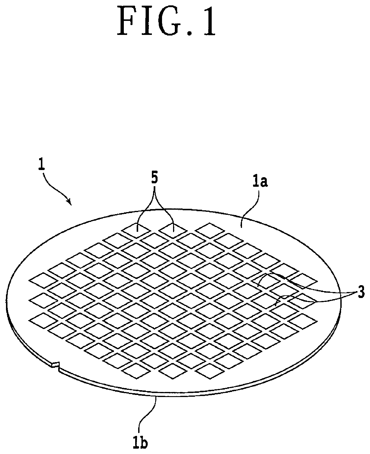
[0030]A preferred embodiment of the present invention will now be described with reference to the attached drawings. There will first be described a wafer to be processed by a wafer processing method according to this preferred embodiment. FIG. 1 is a schematic perspective view of a wafer 1. The wafer 1 is a substantially disc-shaped substrate formed of a material such as silicon (Si), silicon carbide (SiC), gallium nitride (GaN), and gallium arsenide (GaAs). The wafer 1 may be formed of any other semiconductor materials. Further, the wafer 1 may be formed of a material such as sapphire, glass, and quartz. Examples of the glass include alkaline glass, nonalkaline glass, soda lime glass, lead glass, borosilicate glass, and silica glass. The wafer 1 has a front side 1a and a back side 1b. A plurality of crossing division lines 3 are formed on the front side 1a of the wafer 1 to thereby define a plurality of respective separate regions where a plurality of devices 5 such as ICs, LSIs, ...


PUM

PropertyMeasurementUnit
Temperatureaaaaaaaaaa

Abstract

A wafer processing method includes a polyester sheet providing step of positioning a wafer in an inside opening of a ring frame and providing a polyester sheet on a back side of the wafer and on a back side of the ring frame, a uniting step of heating the polyester sheet as applying a pressure to the polyester sheet to thereby unite the wafer and the ring frame through the polyester sheet by thermocompression bonding, a dividing step of applying a laser beam to the wafer to form division grooves in the wafer, thereby dividing the wafer into individual device chips, and a pickup step of blowing air to each device chip through the polyester sheet to push up each device chip, thereby picking up each device chip from the polyester sheet after performing the dividing step.

Description

BACKGROUND OF THE INVENTIONField of the Invention[0001]The present invention relates to a wafer processing method for dividing a wafer along a plurality of division lines to obtain a plurality of individual device chips, the division lines being formed on the front side of the wafer to thereby define a plurality of separate regions where a plurality of devices are individually formed.Description of the Related Art[0002]In a fabrication process for device chips to be used in electronic equipment such as mobile phones and personal computers, a plurality of crossing division lines (streets) are first set on the front side of a wafer formed of a semiconductor, for example, thereby defining a plurality of separate regions on the front side of the wafer. In each separate region, a device such as an integrated circuit (IC), a large-scale integrated circuit (LSI), and a light emitting diode (LED) is next formed. Thereafter, a ring frame having an inside opening is prepared, in which an adhe...

Claims


Application Information

Patent Timeline
IPC IPC(8): H01L21/02H01L21/447H01L21/20H01L21/768
CPCH01L21/76894H01L21/2007H01L21/447H01L21/02013H01L21/78H01L21/6836H01L21/67115H01L2221/68327H01L2221/68386H01L21/67132H01L21/6838H01L21/67092H01L21/76H01L21/324H01L21/185H01L21/50H01L21/2636H01L21/67098H01L21/67248H01L21/67712H01L21/67721B23K26/38H01L2924/061H01L2924/01014H01L2924/1033H01L2924/10329
Inventor HARADA, SHIGENORIMATSUZAWA, MINORUKIUCHI, HAYATOYODO, YOSHIAKIARAKAWA, TAROAGARI, MASAMITSUKAWAMURA, EMIKOFUJII, YUSUKEMIYAI, TOSHIKIOHMAE, MAKIKO
Owner DISCO CORP
Why Eureka
Try Eureka