Wafer transfer blade

Inactive Publication Date: 2009-10-08
APPLIED MATERIALS INC
View PDF9 Cites 344 Cited by
  • Summary
  • Abstract
  • Description
  • Claims
  • Application Information

AI Technical Summary

Benefits of technology

[0021]According to the present invention, the wafer transfer b

Problems solved by technology

This causes impurities to adhere on the

Method used


Image

  • Wafer transfer blade
  • Wafer transfer blade
  • Wafer transfer blade

Examples


Embodiment Construction

[0031]The preferred embodiments of the present invention will now be described in detail with reference to the attached drawings. The same or equivalent similar elements are denoted by the same reference numerals and the overlapped explanation is omitted.

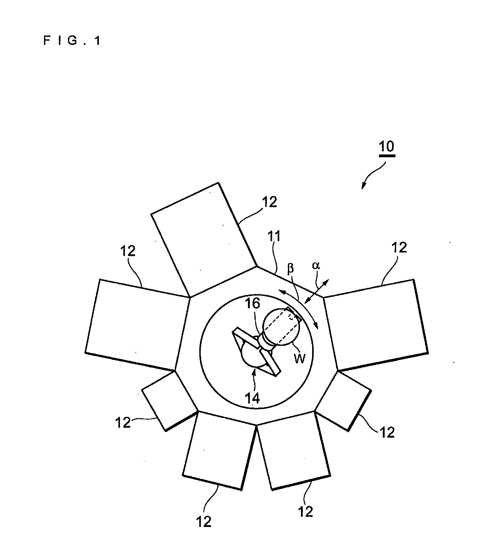
[0032]As shown in FIG. 1, a cluster tool 10 in accordance with an embodiment of the present invention includes a transfer chamber 11 and a plurality of processing chambers 12 radially disposed around the transfer chamber 11. The transfer chamber 11 is provided with a transfer robot 14 to facilitate transfer of a wafer W between the processing chambers 12.

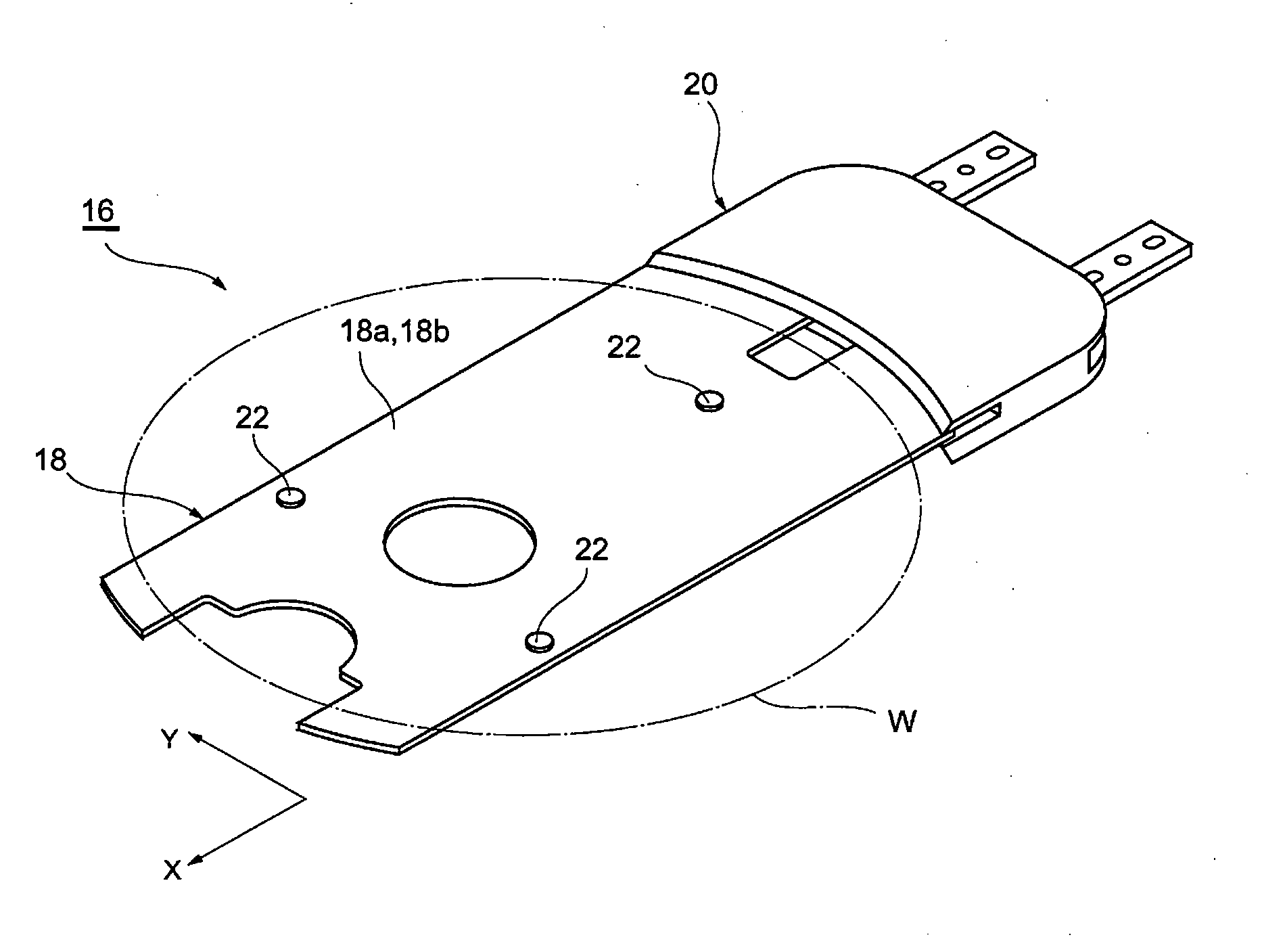
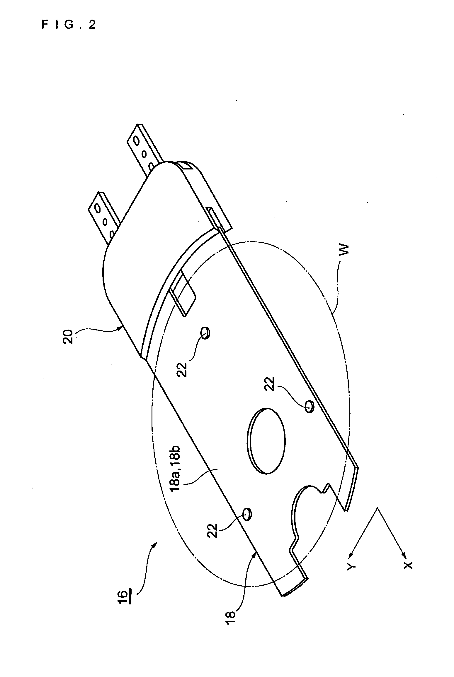
[0033]A blade 16 (wafer transfer blade), which transfers the wafer W (for example, silicon wafer having a diameter of 200 mm), is attached to the transfer robot 14. The transfer robot 14 moves the blade 16 in a direction away from and close to each processing chamber 12 (direction α in FIG. 1) and in a direction between the processing chambers 12 (direction β in FIG. 1).

[0034]As sho...


PUM


Abstract

Projections 22 of the blade 16 provided on a blade surface in a wafer-loading region 18b of a body 18 support a wafer W loaded on the blade surface 18a. Since the projections 22 have microgrooves formed by surface roughening the wafer W is retained on the projections 22 with a suppressed displacement. The blade 16 has a simple structure that retains the wafer W without vacuum suction and has no receiving hole to retain the wafer W in the body 18 of the blade 16. This can effectively prevent formation of defects on the wafer W.

Description

BACKGROUND OF THE INVENTION[0001]1. Field of the Invention[0002]The present invention relates to a wafer transfer blade used in a semiconductor manufacturing device.[0003]2. Description of the Related Art[0004]A wafer transfer blade used in a semiconductor manufacturing device has required high-precision alignment. For example, a vacuum sucking blade, which sucks in the back surface of a wafer with a vacuum chuck to retain the wafer, is known.[0005]A typical known blade for use in vacuum is a flat plate blade provided with a wafer-receiving hole. The wafer-receiving hole is designed such that the diameter of the wafer-receiving hole is slightly greater than that of a wafer to be loaded, and regulates displacement of the wafer on the side face of the wafer-receiving hole (Japanese Unexamined Patent Application Publication Nos. 2001-53135 and 6-181252).[0006]However, this conventional blade has the following problems. Since the vacuum sucking blade is provided with a vacuum device, it...

Claims


Application Information

Patent Timeline
IPC IPC(8): H01L21/67
CPCH01L21/68707
Inventor AOKI, YUJI
Owner APPLIED MATERIALS INC
Why Eureka
Try Eureka