
Level shifter and circuit using the same
- Summary
- Abstract
- Description
- Claims
- Application Information
AI Technical Summary
Benefits of technology
Problems solved by technology
Method used
Image

Examples
Embodiment Construction
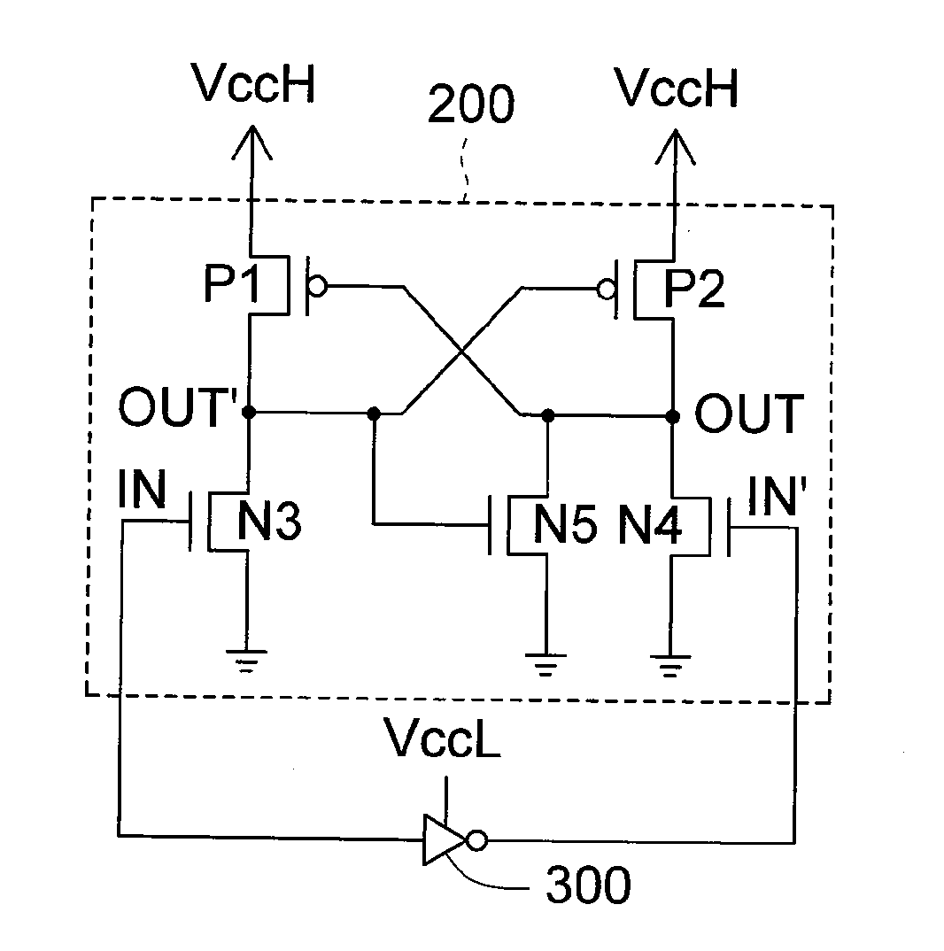
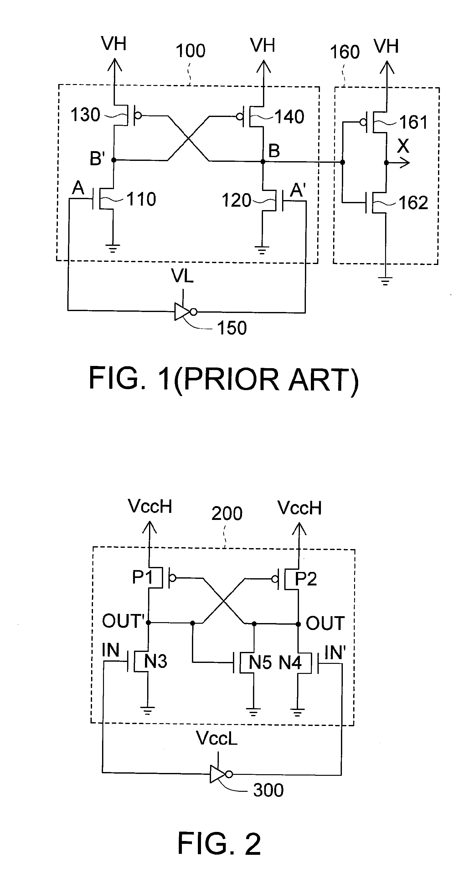
[0023]FIG. 2 is a circuit diagram showing a level shifter 200 and its logic unit according to an embodiment of the invention. Referring to FIG. 2, the level shifter 200 is consisted of transistors P1, P2, N3, N4 and N5. The first ends of the transistors P1 and P2 are coupled to a first supply voltage VccH.
[0024]The control ends of the transistors N3 and N4 respectively receive input signals IN and IN′. The first end of the transistor N3 is coupled to the control end of the transistor P2. The first end of the transistor N4 is coupled to the control end of the transistor P1. The first ends of the transistors N3 and N4 are respectively coupled to the second ends of the transistors P1 and P2. The second ends of the transistors N3 and N4 are coupled to a second supply voltage. In this embodiment, the second supply voltage is a ground voltage. The first end of the transistor N3 outputs an output signal OUT′. The first end of the transistor N4 outputs an output signal OUT.
[0025]The first e...
PUM
 Abstract
Description
Claims
Application Information