Low Noise Amplifier With Noise And Linearity Improvement
- Summary
- Abstract
- Description
- Claims
- Application Information
AI Technical Summary
Benefits of technology
Problems solved by technology
Method used
Image
Examples
Embodiment Construction
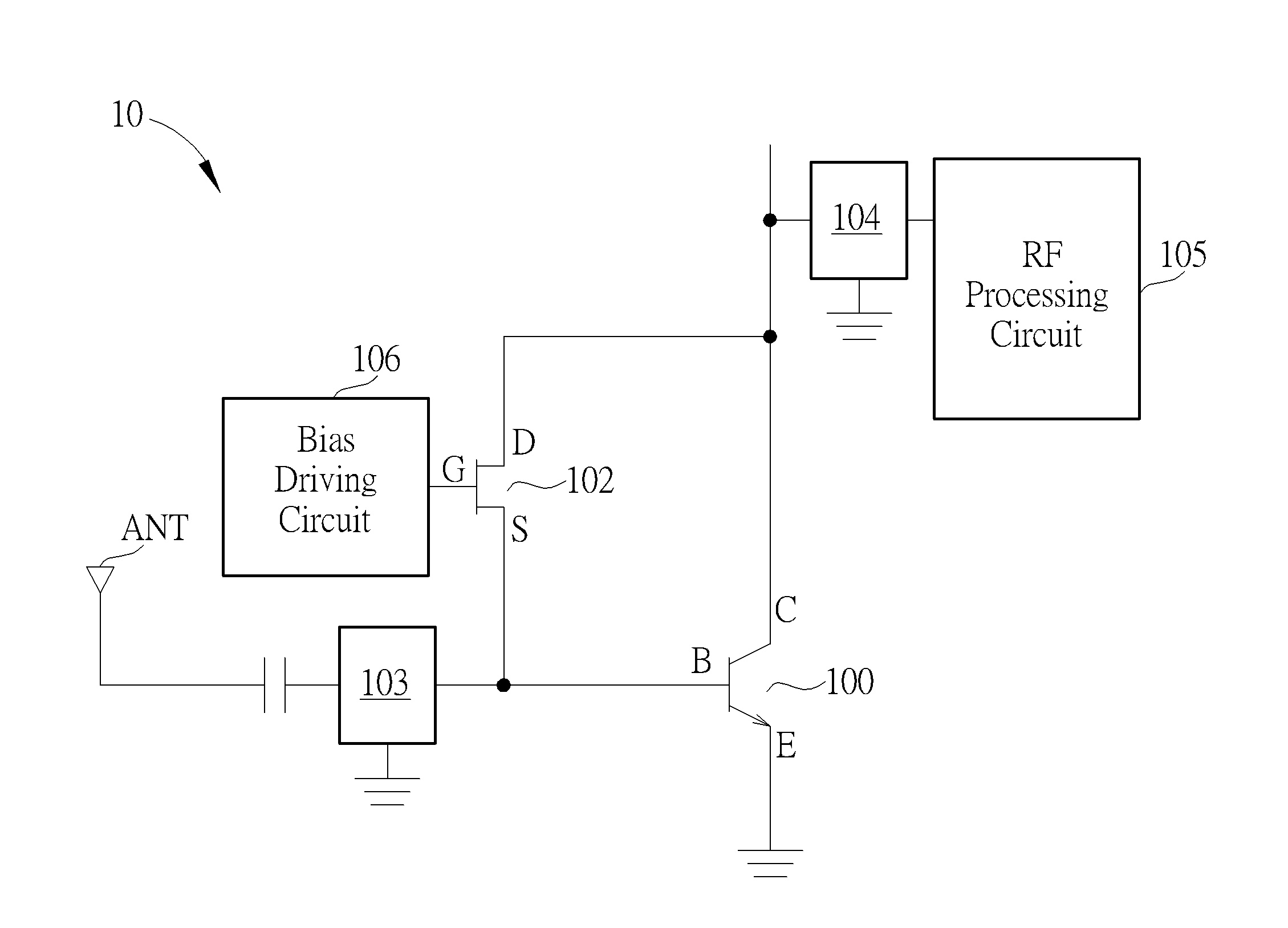
[0017]FIG. 1 is a schematic diagram of a low noise amplifier 10 according to an embodiment of the present invention. The low noise amplifier 10 comprises an amplifying transistor 100 and an auxiliary transistor 102. The amplifying transistor 100 may be a bipolar junction transistor (BJT) or a heterojunction bipolar transistor (HBT). The auxiliary transistor 102 may be a metal-oxide-semiconductor field effect transistor (MOSFET) or a high electron mobility transistor (HEMT). The amplifying transistor 100 comprises a base B (first terminal), a collector C (second terminal) and an emitter E (third terminal). The base B is coupled to an antenna ANT. The base B may be coupled to the antenna ANT through an input network 103, wherein the input network 103 may comprise an impedance matching network or a band pass filter (not illustrated in FIG. 1). The base B is utilized to receive an input signal of the low noise amplifier 10. The collector C is coupled to a radio frequency processing circ...
PUM
 Abstract
Description
Claims
Application Information


