Pixel and organic light emitting display device

a technology of light-emitting display device and pixel, which is applied in the direction of lighting devices, light sources, instruments, etc., can solve the problem that the desired voltage cannot be precisely charged in the storage capacitor, and achieve the effect of saving manufacturing costs

Active Publication Date: 2009-10-08
SAMSUNG DISPLAY CO LTD
View PDF3 Cites 13 Cited by
  • Summary
  • Abstract
  • Description
  • Claims
  • Application Information

AI Technical Summary

Benefits of technology

[0014]In a pixel and an organic light emitting display device using the same according to the present invention, since the voltage of a gate electrode of a driving transistor is raised using a boosting capacitor, an image with a desired gray level can be displayed. Further, in accordance with the present invention, since a storage capacitor and a boosting capacitor are formed as MOS capacitors, manufacturing costs can be saved.

Problems solved by technology

Recently, there have been various types of flat panel display devices capable of reducing their weight and volume, which are unfavorable in cathode ray tubes.
However, in a conventional organic light emitting display device, a desired voltage may not be precisely charged in the storage capacitor.

Method used


Image

  • Pixel and organic light emitting display device
  • Pixel and organic light emitting display device
  • Pixel and organic light emitting display device

Examples


Embodiment Construction

[0019]Hereinafter, when a first element is described as being coupled to a second element, the first element may not only be directly coupled to the second element but may also be indirectly coupled to the second element via a third element. Further, some of the elements that are not essential to the complete understanding of the invention are omitted for clarity. Also, like reference numerals refer to like elements throughout.

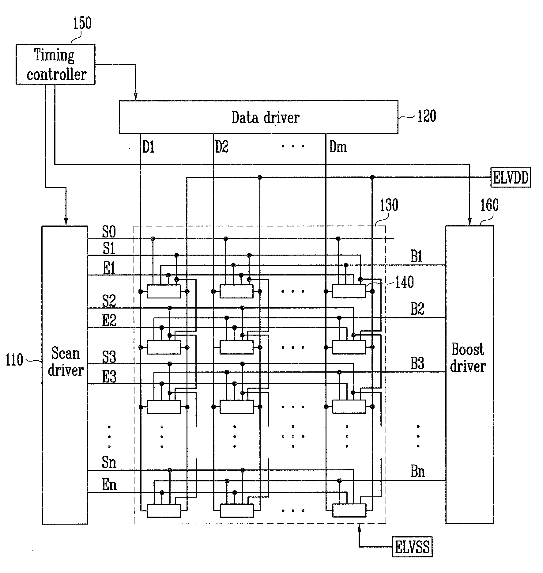
[0020]Referring to FIG. 1, the organic light emitting display device according to the embodiment of the present invention includes a scan driver 110, a data driver 120, a pixel unit 130, a timing controller 150, and a boost driver 160.

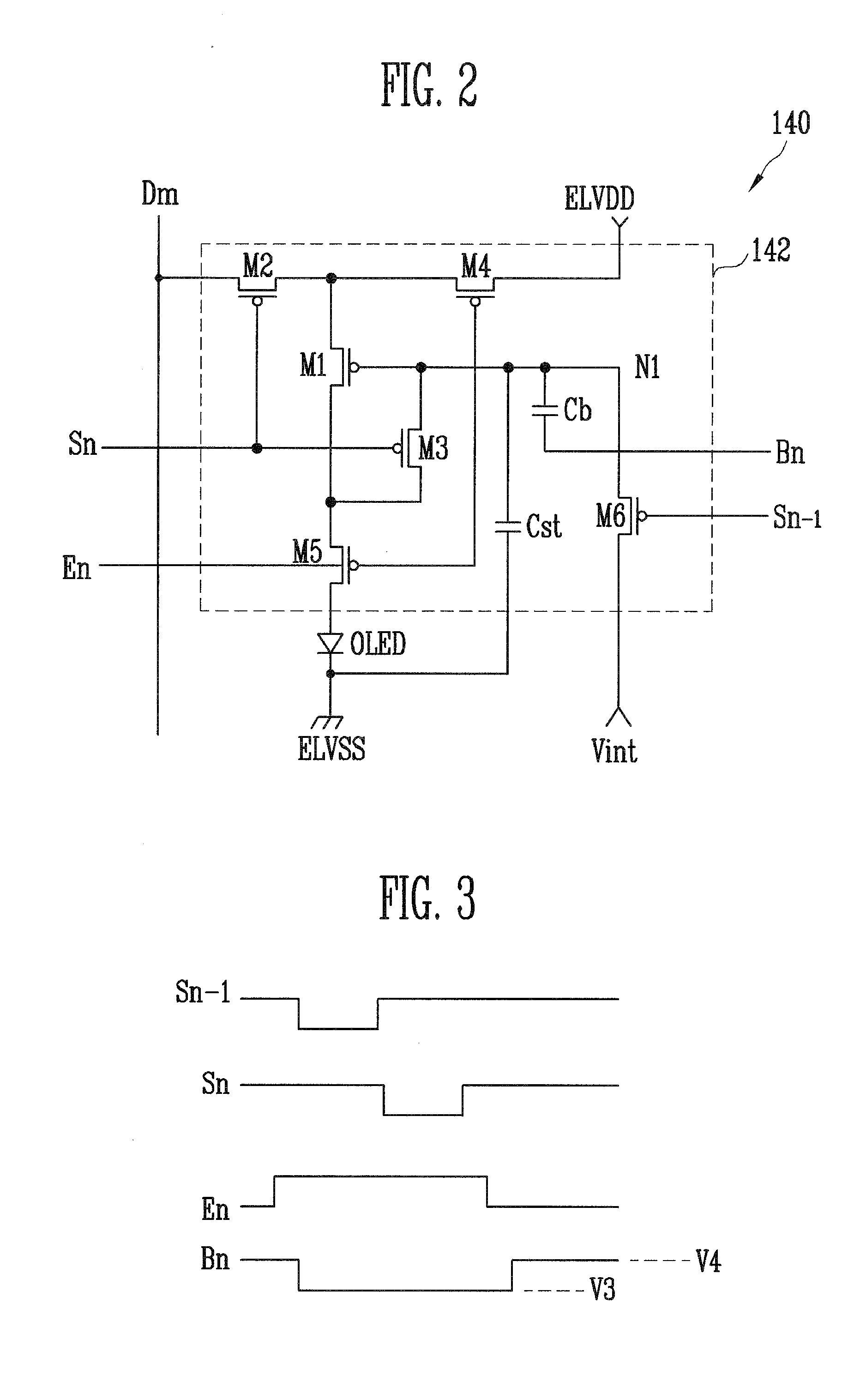
[0021]The pixel unit 130 includes a plurality of pixels 140 positioned at regions defined by scan lines S1 to Sn, light emitting control lines E1 to En, boost lines B1 to Bn and data lines D1 to Dm. Each of the pixels 140 emits light with a predetermined luminance in response to a data signal supplied from a data line D.

[0022]To ...


PUM


Abstract

A pixel and an organic light emitting display device using the same is provided. The pixel includes an organic light emitting diode (OLED). A pixel circuit controls an amount of current that flows into the OLED. In the pixel, the pixel circuit includes a first transistor controlling an amount of current that flows into a second power source via the OLED from a first power source. A storage capacitor is positioned between a gate electrode of the first transistor and the second power source. A boosting capacitor is positioned between the gate electrode of the first transistor and a boost line.

Description

CROSS-REFERENCE TO RELATED APPLICATION[0001]This application claims priority to and the benefit of Korean Patent Application No. 10-2008-0031089, filed on Apr. 3, 2008, in the Korean Intellectual Property Office, the entire content of which is incorporated herein by reference.BACKGROUND OF THE INVENTION[0002]1. Field of the Invention[0003]The present invention relates to a pixel and an organic light emitting display device using the same, and more particularly, to a pixel and an organic light emitting display device using the same that can save manufacturing costs and stably express a black gray level.[0004]2. Description of Related Art[0005]Recently, there have been various types of flat panel display devices capable of reducing their weight and volume, which are unfavorable in cathode ray tubes. The flat panel display devices include, for example, liquid crystal displays, field emission displays, plasma display panels and organic light emitting display devices.[0006]Among these fl...

Claims


Application Information

Patent Timeline
Patent Type & Authority Applications(United States)
IPC IPC(8): G09G3/30
CPCG09G3/3233G09G3/3266G09G2300/0819G09G2300/0852G09G2320/0238G09G2310/0262G09G2310/0275G09G2320/0223G09G2300/0861G09G3/20G09G3/30G09G3/32H05B33/12
Inventor KIM, DONG-HWIKIM, YANG-WAN
Owner SAMSUNG DISPLAY CO LTD
Why Eureka
Try Eureka