Solid-state image capturing apparatus and electronic information equipment

a technology of solid-state image and electronic information equipment, which is applied in the direction of color television details, television system details, television system noise, etc., can solve the problems of increasing the chip area and the current consumption, affecting and affecting the noise of the driver transistor output side, so as to reduce the decrease of the pixel source voltage, stable voltage level to the pixels, and the effect of preventing the influence of noise on the output side of the driver transistor

Active Publication Date: 2009-10-08
SHARP KK
View PDF2 Cites 34 Cited by
  • Summary
  • Abstract
  • Description
  • Claims
  • Application Information

AI Technical Summary

Benefits of technology

[0045]According to the present invention, a power supply circuit for stepping down an external source voltage to generate a pixel source voltage to be supplied to each pixel in a pixel array is provided; and the power supply circuit is configured to include a driver transistor for generating the pixel source voltage from the external source voltage, the driver transistor being operative in a saturated state. As a result, even when noise is superimposed on the external source voltage, the influence of the noise to the output side of the driver transistor can be prevented.
[0046]Further, according to the present invention, a bias level generating circuit for creating aconstant bias level based on a reference signal is provided; and the bias level is used as a control voltage of a driver transistor that constitutes the power supply circuit. Consequently, the pixel source voltage supplied from the power supply circuit to the pixel can be maintained constant.
[0048]Further, according to the present invention, a plurality of driver transistors that constitute the power supply circuit are positioned along one edge of the pixel array, so that it is possible to reduce the decrease of the pixel source voltage supplied to the pixel due to the wiring resistance in the pixel area depending on the location of the pixel column in the pixel array.
[0049]Further, according to the present invention, a single depletion NMOS transistor is provided as a driver transistor that constitutes the power supply circuit, so that the area occupied by a transistor can be small in the power supply circuit and the layout for positioning circuit elements can have enough room in reserve.
[0050]Further, according to the present invention, a negative voltage generating circuit for generating a negative voltage based on the reference signal is provided, and a negative voltage generated at the negative voltage generating circuit is applied to a pixel section P-well area including an anode area of the photodiode, so that the decrease of the pixel source voltage from the external source voltage at the power supply circuit can be compensated.
[0051]As described above, according to the present invention, the power supply circuit for stepping down the external source voltage to generate the pixel source voltage to be supplied to each pixel in the pixel array is provided, and the power supply circuit is configured to include a driver transistor for generating the pixel source voltage from the external source voltage, the driver transistor being operative in a saturated state. As a result, even when noise is superimposed on the external source voltage, the influence of the noise to the output side of the driver transistor can be prevented, which results in obtaining an effect to supply a stable voltage level to the pixels and further the vertical driving circuit without using a boosting circuit that causes an increase in the layout area and the current consumption.

Problems solved by technology

As described above, when the source voltage, supplied from the outside of the chip, is directly inputted into the pixel and the vertical driving circuit, horizontal line noise occurs due to the influence of the noise superimposed from the source voltage.
Further, when a boosting circuit is used for the pixel and the power source of the vertical driving circuit in order to prevent this problem, other significant problems, such as the increase of the chip area and the increase of the current consumption, occur.

Method used


Image

  • Solid-state image capturing apparatus and electronic information equipment
  • Solid-state image capturing apparatus and electronic information equipment
  • Solid-state image capturing apparatus and electronic information equipment

Examples


embodiment 1

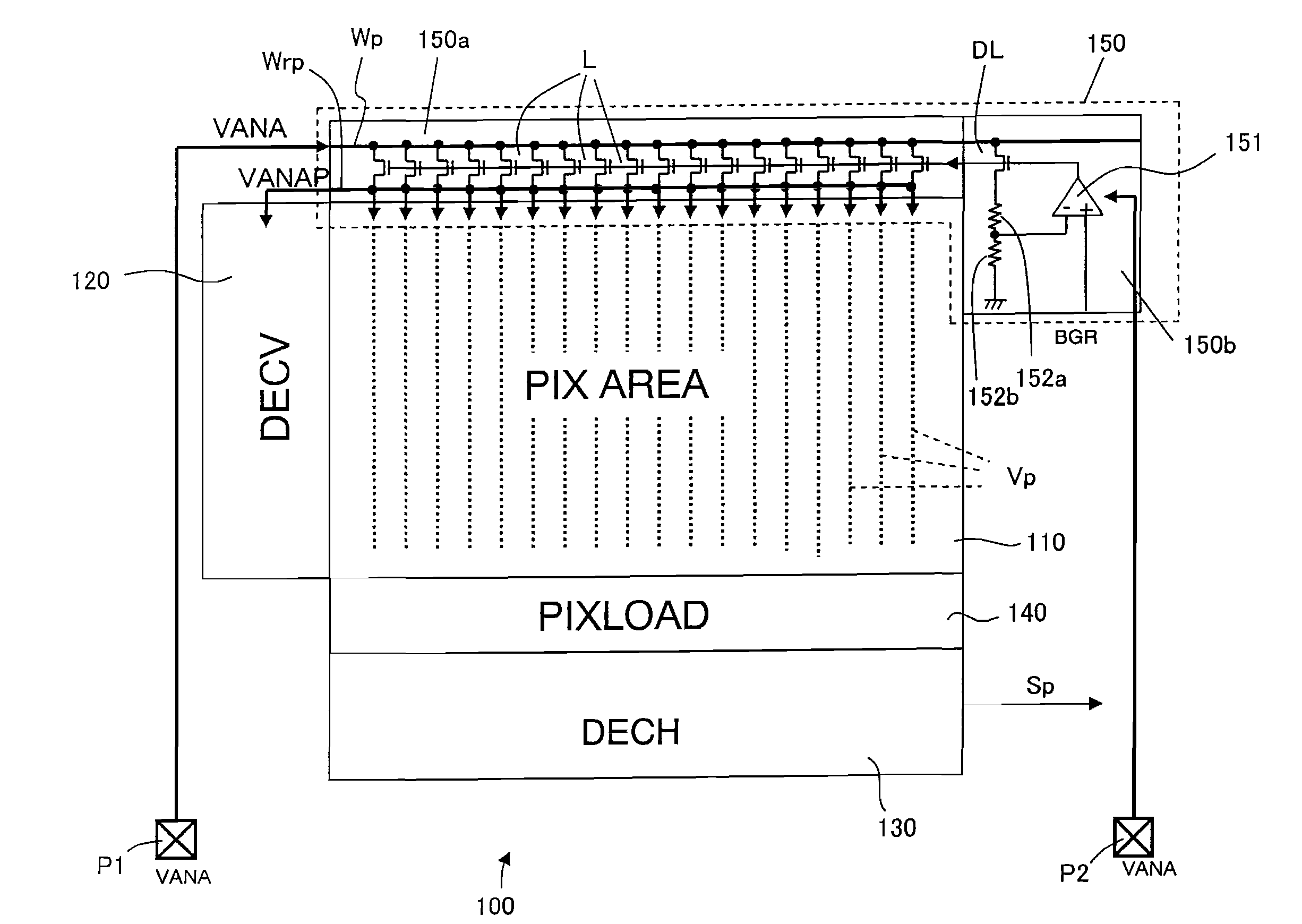
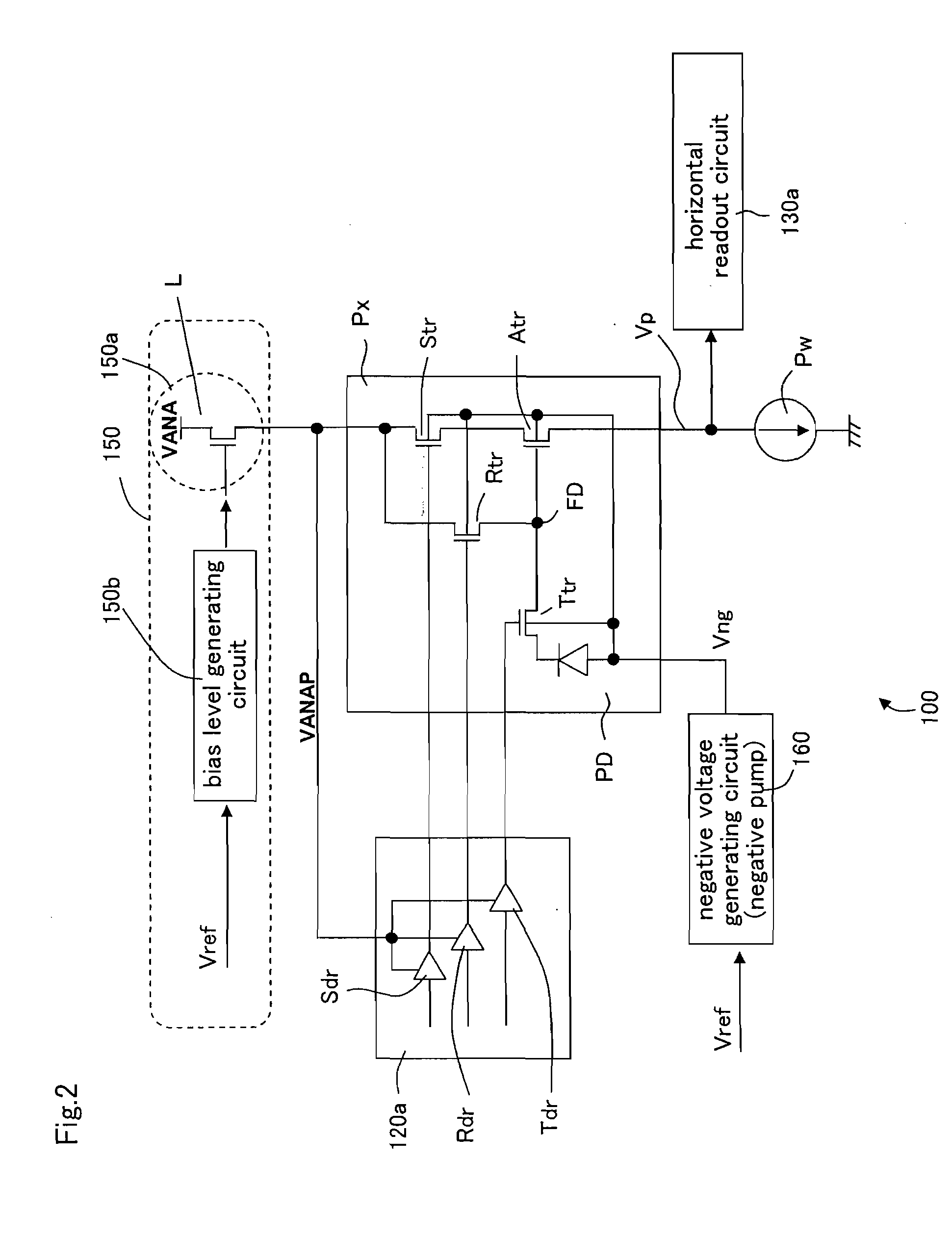
[0082]FIG. 1 is a block diagram illustrating a solid-state image capturing apparatus according to Embodiment 1 of the present invention, showing a configuration for supplying an external source voltage to pixels and a vertical driving circuit.

[0083]A solid-state image capturing apparatus 100 according to Embodiment 1 is the conventional solid-state image capturing apparatus 200 shown in FIG. 6 equipped with a pixel power source regulator 150 for stepping down a source voltage VANA from an external power source to generate a constant level of pixel source voltage (analog voltage) VANAP.

[0084]That is, the solid-state image capturing apparatus 100 includes a pixel array (PIX AREA) 110 where pixels are arranged in a matrix; a vertical signal line (output signal line Vp provided to correspond to each pixel column of the pixel array for reading out a voltage signal from each pixel of a corresponding pixel column; a vertical scanning circuit (DECV) 120 for selecting a specific pixel row in...

embodiment 2

[0120]FIG. 4 is a block diagram illustrating a solid-state image capturing apparatus according to Embodiment 2 of the present invention, showing a configuration for supplying an external source voltage to a pixel and a vertical driving circuit.

[0121]A solid-state image capturing apparatus 100a according to Embodiment 2 is configured with a pixel power source regulator 170 that includes a pixel power source driver 170a consisting of a single driver transistor, instead of the pixel power source regulator 150 of the solid-state image capturing apparatus 100 according to Embodiment 1.

[0122]In the solid-state image capturing apparatus 100a according to Embodiment 2 with the configuration described above, the current supply capability of the pixel power source driver transistor Lt, which creates a pixel voltage VANAP based on the reference voltage (PIX_SFGATE) generated in the pixel source regulator 170, is increased (the transistor width is increased) so as to supply the pixel source vol...

embodiment 3

[0124]FIG. 5 is a block diagram illustrating a solid-state image capturing apparatus according to Embodiment 3 of the present invention, showing a configuration for supplying an external source voltage to a pixel and a vertical driving circuit.

[0125]A solid-state image capturing apparatus 100b according to Embodiment 3 is configured with a pixel Py with a 3Tr configuration instead of the pixel Px with a 4Tr configuration that constitutes the pixel array of the solid-state image capturing apparatus 100 according to Embodiment 1 described above.

[0126]That is, the pixel Py that constitutes the pixel array includes: a photoelectric conversion element (photodiode) PD; an electric charge accumulating section (floating diffusion) FD for accumulating the signal charge generated at the photodiode PD; a transfer transistor Ttr for transferring the signal charge generated at the photodiode to the electric charge accumulating section FD; a reset transistor Rtr for resetting the signal charge ac...


PUM


Abstract

A solid-state image capturing apparatus according to the present invention includes: a pixel array in which a plurality of pixels are arranged; a driving circuit for driving each pixel of the pixel array; and a power supply circuit for stepping down an external source voltage supplied from an external power source to generate a pixel source voltage to be supplied to each pixel of the pixel array, where the power supply circuit includes a driver transistor for generating a pixel source voltage from the external source voltage and the driver transistor is operative in a saturated state.

Description

[0001]This nonprovisional application claims priority under 35 U.S.C. §119(a) to Patent Application No. 2008-097617 filed in Japan on Apr. 3, 2008, the entire contents of which are hereby incorporated by reference.BACKGROUND OF THE INVENTION[0002]1. Field of the Invention[0003]The present invention relates to a solid-state image capturing apparatus and an electronic information equipment, and in particular, to a solid-state image capturing apparatus equipped with a pixel power regulator and an electronic information equipment using such a solid-state image capturing apparatus.[0004]2. Description of the Related Art[0005]In conventional solid-state image capturing apparatuses, an external source voltage VANA, which is supplied from the outside of the chips that constitute the solid-state image capturing apparatus, is generally used as voltage to be supplied to pixels.[0006]FIG. 6 is a block diagram illustrating a conventional solid-state image capturing apparatus, showing a configura...

Claims


Application Information

Patent Timeline
Patent Type & Authority Applications(United States)
IPC IPC(8): H04N5/335H04N5/357H04N5/369H04N5/374H04N5/376
CPCH04N5/3658H04N5/335H04N25/00H04N25/677
Inventor HATTORI, SHINJITSUJI, KIYOSHIGE
Owner SHARP KK
Why Eureka
Try Eureka