Semiconductor light emitting element and method for manufacturing same

a technology of semiconductors and light emitting elements, applied in the direction of semiconductor/solid-state device manufacturing, semiconductor devices, electrical devices, etc., to achieve the effect of suppressing leakage current and preventing an increase in drive voltag

Active Publication Date: 2009-10-15
ROHM CO LTD
View PDF15 Cites 7 Cited by
  • Summary
  • Abstract
  • Description
  • Claims
  • Application Information

AI Technical Summary

Benefits of technology

[0008]The present invention has been proposed under the circumstances described above. It is, therefore, an object of the present invention to provide a semiconductor light emitting element which is capable of preventing an increase in drive voltage and suppressing leakage current.
[0010]This arrangement provides the following technical effects. In the process of etching the insulating layer after the n-side electrode and the p-side electrode are formed, only the second layer of each electrode is subjected to the etching. Since the second layer is made of Ni, W, Zr or Pt, the surface is not considerably damaged by the etching. Thus, the resistance at the interface between each electrode and the member electrically connected to the electrode is relatively low. Thus, the semiconductor light emitting element can be driven at a relatively low voltage. Further, in each of the electrodes, the upper surface of the first layer can be entirely covered by the second layer. In this case, of each electrode, the portion which is in contact with the insulating layer mostly comprises the second layer. (For instance, this state can be provided by making the first layer appropriately thin.) Ni, W, Zr or Pt which forms the second layer is unlikely to diffuse into the insulating layer, as compared with Au. Thus, the insulating layer 7 does not unduly become conductive, whereby leakage current in the semiconductor light emitting element is prevented.
[0011]Preferably, the semiconductor light emitting element further comprises a wiring contacting the n-side electrode (or the p-side electrode). The wiring includes a first layer, and a second layer formed on the first layer. The first layer of the wiring is in contact with the second layer of the n-side electrode (or the p-side electrode) and made of the same material as that of the second layer of the n-side electrode (or the p-side electrode). The second layer of the wiring is made of Au. With this arrangement, the n-side electrode or the p-side electrode and the wiring are bonded to each other at the portions made of the same material. With this arrangement, the resistance at the interface between each electrode and the wiring is lower as compared with the structure in which different kinds of metals are bonded to each other.
[0013]With this arrangement, only the second layer of each of the n-side electrode and the p-side electrode is subjected to etching. Since the second layer is made of Ni, W, Zr or Pt, the surface is not considerably damaged by the etching. Thus, the resistance at the interface between each of the n-side electrode and the p-side electrode and the member electrically connected to the electrode is relatively low. This makes it possible to drive the semiconductor light emitting element at a relatively low voltage.

Problems solved by technology

However, this arrangement causes another problem.

Method used


Image

  • Semiconductor light emitting element and method for manufacturing same
  • Semiconductor light emitting element and method for manufacturing same
  • Semiconductor light emitting element and method for manufacturing same

Examples


Embodiment Construction

[0025]Preferred embodiments of the present invention will be described below with reference to the accompanying drawings.

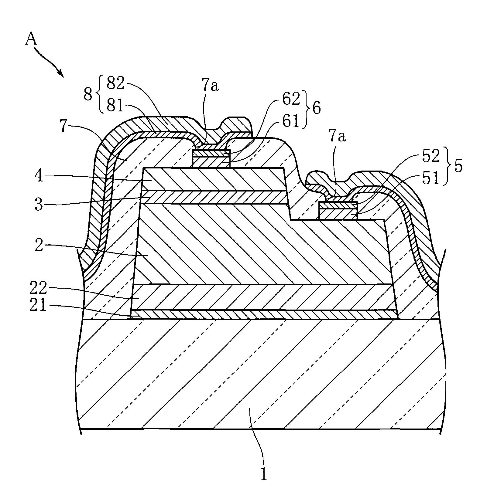
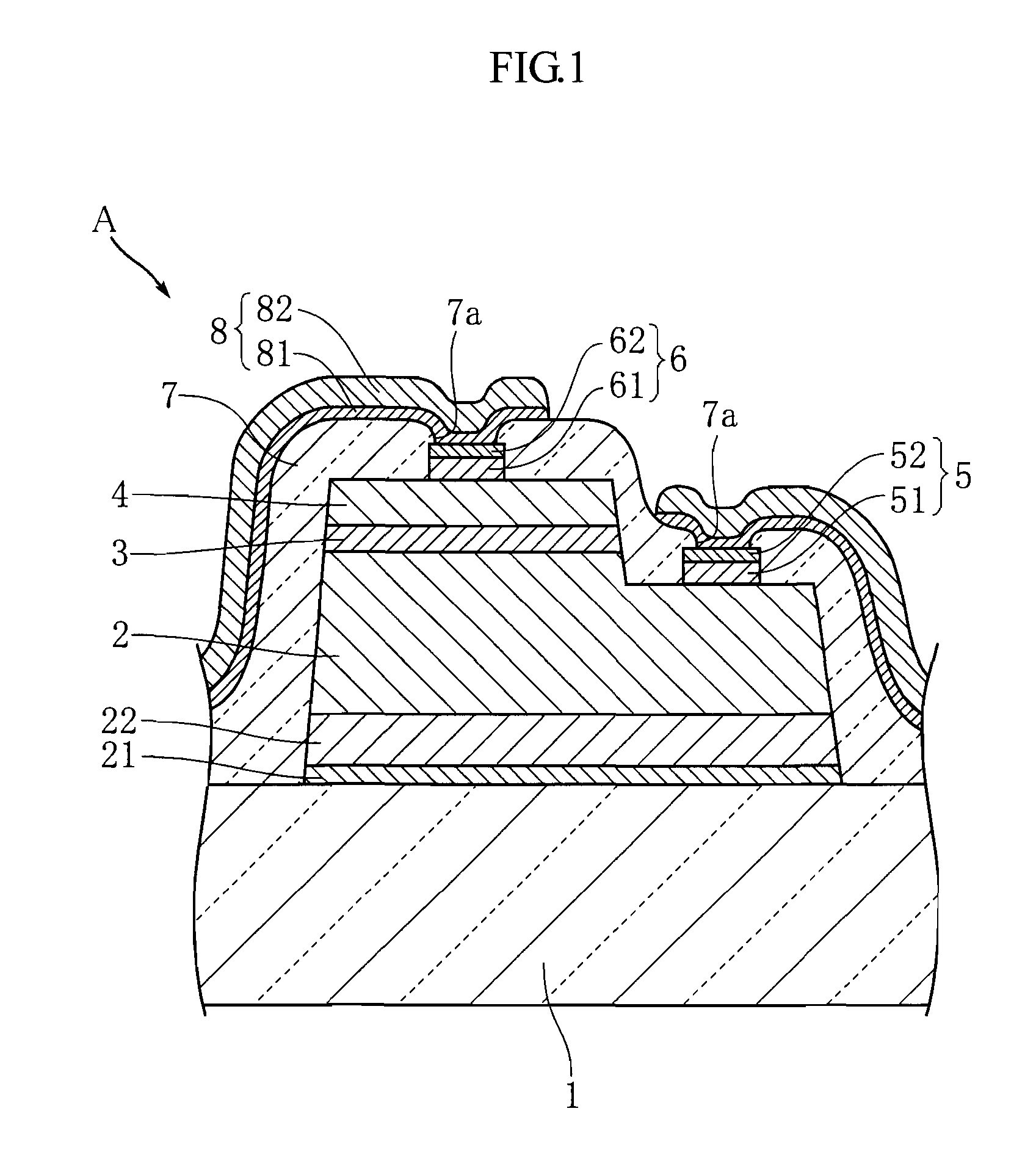
[0026]FIG. 1 shows an example of semiconductor light emitting element according to the present invention. The illustrated semiconductor light emitting element A is formed on a substrate 1 and includes an n-GaN layer 2, an active layer 3, a p-GaN layer 4, an n-side electrode 5, a p-side electrode 6, an insulating layer 7 and a wiring 8. The semiconductor light emitting element A is designed to emit light through the insulating layer 7.

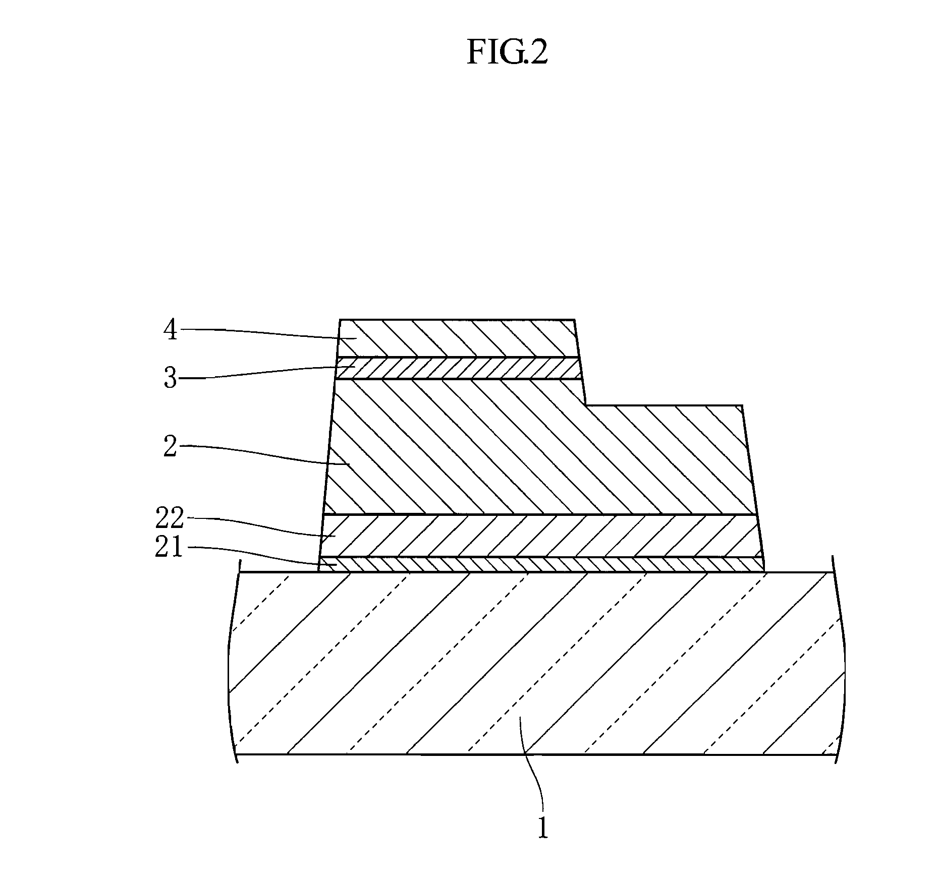
[0027]The substrate 1 is made of e.g. sapphire and supports the n-GaN layer 2, the active layer 3, the p-GaN layer 4 and so on. The substrate 1 has a thickness of e.g. about 350 μm.

[0028]The n-GaN layer 2 is a layer formed by doping Si into GaN. The n-GaN layer 2 has a thickness of e.g. about 3.5 μm. A buffer layer 21 and an undoped GaN layer 22 are laminated between the substrate 1 and the n-GaN layer 2. The buffer layer 21 and the u...


PUM


Abstract

A semiconductor light emitter (A) includes an n-type semiconductor layer (2), a p-type semiconductor layer (4), and an active layer (3) between these two layers (2, 4). The light emitter (A) further includes an n-side electrode (5) on the n-type layer (2) and a p-side electrode (6) on the p-type layer (4). An insulating layer (7) covers the n-type and p-type layers (2),(4), while also partially covering the n-side and p-side electrodes (5),(6), leaving part of the electrodes (5, 6) exposed. The n-side electrode (5) has a first Al layer (51) formed on the n-type layer (2) and a second Ni, W, Zr or Pt layer (52) formed on the first layer (51). The p-side electrode (6) has a first Au layer (61) formed on the p-type layer (4), and a second Ni, W, Zr or Pt layer (62) formed on the first layer (61).

Description

TECHNICAL FIELD[0001]The present invention relates to a semiconductor light emitting element and a method for manufacturing the same. BACKGROUND ART[0002]Semiconductor lasers or light emitting diodes are examples of conventional semiconductor light emitting elements (see e.g. Patent Document 1 below). Semiconductor light emitting elements can provide in general high luminance with less power consumption, thereby making a suitable light source for a liquid crystal display device, for example.[0003]Patent Document 1: JP-A-2003-243773[0004]FIG. 10 shows a conventional semiconductor light emitting element. The illustrated light emitting element X includes a substrate 101, on which an n-GaN layer 102, an active layer 103 and a p-GaN layer 104 are laminated. The n-GaN layer 102 and the p-GaN layer 104 are covered by an insulating layer 107. The insulating layer 107 is made of e.g. SiO2 and formed with two openings 107a. The openings 107a expose part of the n-GaN layer 102 and p-GaN layer ...

Claims


Application Information

Patent Timeline
Patent Type & Authority Applications(United States)
IPC IPC(8): H01L33/00H01L21/283H01L33/06H01L33/12H01L33/32H01L33/40
CPCH01L24/18H01L24/82H01L25/0753H01L33/32H01L33/40H01L33/44H01L2224/82007H01L2224/24051H01L2224/24226H01L2224/24998H01L2924/01078H01L2924/01079H01L2924/01012H01L33/62H01L2224/32225H01L2224/73267H01L2224/92244H01L24/24H01L2224/24137
Inventor SHAKUDA, YUKIO
Owner ROHM CO LTD
Why Eureka
Try Eureka