Solar cell lead wire, method of making the same, and solar cell

a solar cell and lead wire technology, applied in the field of solar cell lead wire, can solve the problems of difficult adjustment of the pressure applied to the strip-shaped conducting material, inferior section size accuracy of the concave conducting material, and inferior mass productivity of the process, so as to prevent the cell from cracking

Inactive Publication Date: 2009-10-22
HITACHI METALS LTD
View PDF4 Cites 9 Cited by
  • Summary
  • Abstract
  • Description
  • Claims
  • Application Information

AI Technical Summary

Benefits of technology

[0019]Therefore, it is an object of the invention to provide a solar cell lead wire that can effectively prevent the cell cracking.

Problems solved by technology

Since the plastic forming process and the bending process are an intermittent process, these processes are inferior in mass productivity.
Further, when the strip-shaped conducting material is passed through the molding roll, it is difficult to adjust the pressure applied to the strip-shaped conducting material so that the under concavity conducting material is inferior in accuracy of the section size.
The problem remains, that the cell crack occurs in the semiconductor substrate due to the displacements.
Since most of the solar cell cost is the semiconductor substrate cost. downsizing in thickness of the semiconductor substrate is investigated, but the semiconductor substrate downsized in thickness easily cracks.
The downsizing in thickness of the semiconductor substrate cannot be expected in the situation that the cell crack occurs in the semiconductor substrate due to the solar cell lead wires

Method used


Image

  • Solar cell lead wire, method of making the same, and solar cell
  • Solar cell lead wire, method of making the same, and solar cell
  • Solar cell lead wire, method of making the same, and solar cell

Examples


example 1

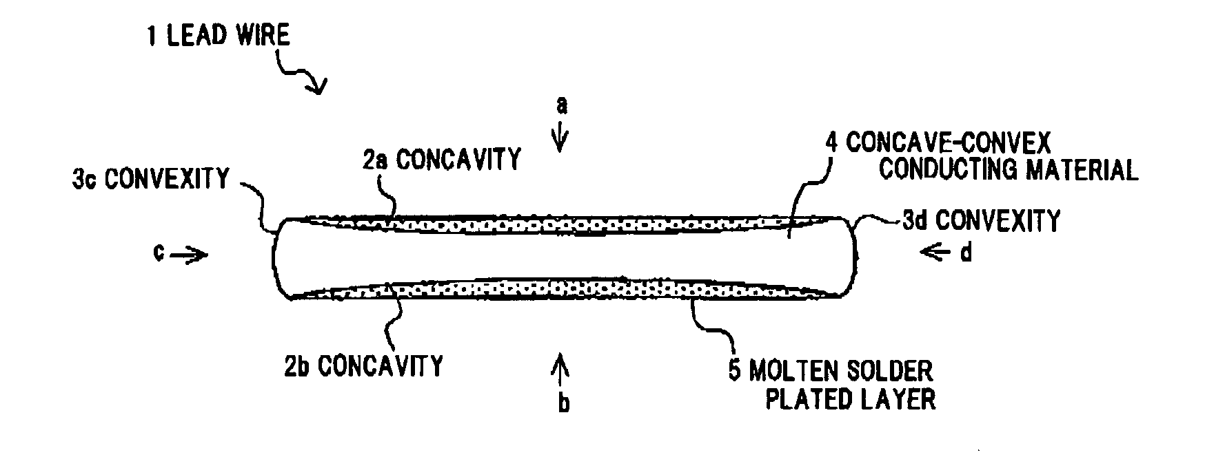
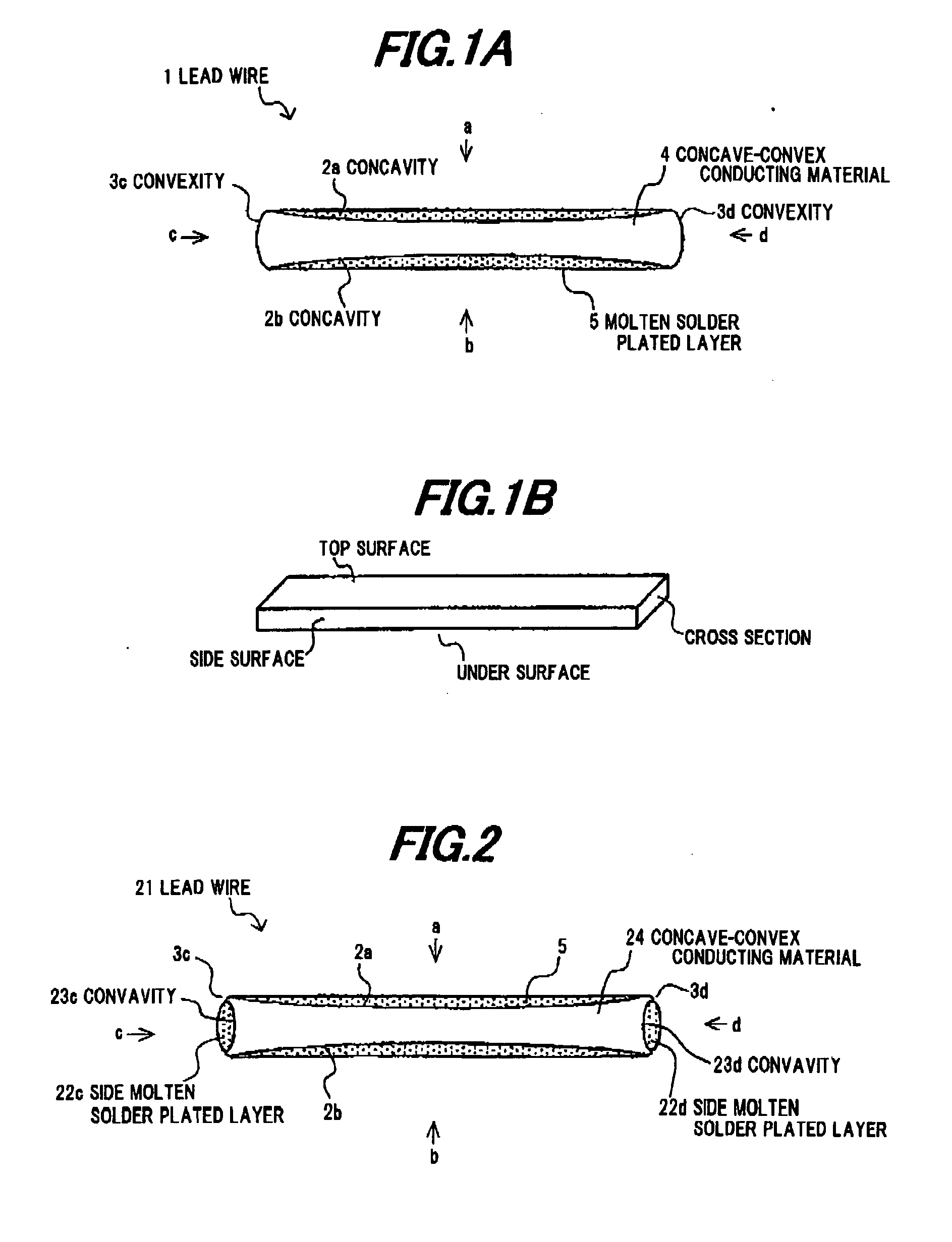
[0102]A strip-shaped conducting material which has a rectangular wire-like shape of 2.0 mm in width and 0.16 mm in thickness was formed by applying a roll processing to a Cu material as a raw conducting material. A concave-convex conducting material 4 having concavities 2a, 2b was formed by applying a drawing or extruding die processing to the strip-shaped conducting material. The concave-convex conducting material 4 was heat-treated by using a batch heating equipment; and molten solder plated layers were formed on the concavities 2a, 2b of the concave-convex conducting material 4 so as to have flat surfaces by coating with solder plating of Sn-3% Ag-0.5Cu around the strip-shaped conducting material 4 (the heat-treated Cu was used as the conducting body). From the above, the solar cell lead wire 1 shown in FIG. 1 was obtained.

example 2

[0103]In addition to the composition of the solar cell lead wire 1 of Example 1, the side molten solder plated layers 22c, 22d were formed on the convexities 3c, 3d on the side surfaces c, d, and the solar cell lead wire 21 shown in FIG. 2 was obtained.

example 3

[0104]A strip-shaped conducting material which has a rectangular wire-like shape of 2.0 mm in width and 0.16 mm in thickness was formed by applying a slit processing to a Cu-invar-Cu material (ratio of 2:1:2) as a raw conducting material. A concave-convex conducting material 4 having concavities 2a, 2b was formed by applying a drawing or extruding die processing to the strip-shaped conducting material. Molten solder plated layers were formed on the concavities 2a, 2b of the concave-convex conducting material 4 so as to have flat surfaces by coating with solder plating around the strip-shaped conducting material 4. From the above, the solar cell lead wire 1 shown in FIG. 1 was obtained.


PUM

PropertyMeasurementUnit
thicknessaaaaaaaaaa
widthaaaaaaaaaa
widthaaaaaaaaaa

Abstract

A solar cell lead wire includes a conducting material, and a molten solder plated layer formed on the conducting material. The conducting material includes a concave-convex conducting material that includes a concavity on top and under surfaces thereof, respectively, and a convexity on a side surface thereof, and that is formed by die processing a strip-shaped conducting material, and the molten solder plated layer comprises a flat surface formed by supplying a molten solder to the concavity of the concave-convex conducting material.

Description

[0001]The present application is based on Japanese patent application Nos.2008-31658 and 2008-288813 filed Feb. 13, 2008 and Nov. 11, 2008, respectively, the entire contents of which are incorporated herein by reference.BACKGROUND OF THE INVENTION[0002]1. Field of the Invention[0003]This invention relates to a solar cell lead wire (i.e., a lead wire for a solar cell) that can effectively prevent cracking in a solar cell caused by a displacement of the lead wire.[0004]2. Description of the Related Art[0005]A polycrystal or single crystal Si cell is used for a semiconductor substrate of a solar cell. As shown in FIG. 4, a solar cell 101 is fabricated by joining solar cell lead wires 103 by soldering to predetermined regions of a semiconductor substrate 102. The solar cell lead wires 103 are joined to a front surface electrode 104 and a rear surface electrode 105 formed on the surface of the semiconductor substrate 102 by soldering. Electricity generated in the semiconductor substrate ...

Claims


Application Information

Patent Timeline
Patent Type & Authority Applications(United States)
IPC IPC(8): H01L31/00H01B5/00B21D31/00
CPCC23C2/02C23C2/08H01L31/0508C23C26/02Y02E10/50C23C6/00C23C2/022
Inventor NISHI, HAJIMEENDO, YUJUAKUTSU, HIROYUKIOKIKAWA, HIROSHI
Owner HITACHI METALS LTD
Why Eureka
Try Eureka