Production of self-organized pin-type nanostructures, and the rather extensive applications thereof

a nanostructure and self-organized technology, applied in the field of pin-type structure production, to achieve the effect of efficient further processing and gain in device performan

Active Publication Date: 2009-10-22
X FAB SEMICON FOUNDRIES
View PDF12 Cites 25 Cited by
  • Summary
  • Abstract
  • Description
  • Claims
  • Application Information

AI Technical Summary

Benefits of technology

[0007]It is an object of the present invention to provide methods and devices wherein nanostructures may be integrated in a reliable and cost-efficient manner while concurrently ensuring an efficient further processing and gain in performance of the devices.

Problems solved by technology

Due to the pronounced difference of the impedances or indices of refraction of air and the semiconductor material, such as silicon, a large number of photons is however reflected at the interface and does not reach the location of the conversion.

Method used


Image

  • Production of self-organized pin-type nanostructures, and the rather extensive applications thereof
  • Production of self-organized pin-type nanostructures, and the rather extensive applications thereof
  • Production of self-organized pin-type nanostructures, and the rather extensive applications thereof

Examples


Embodiment Construction

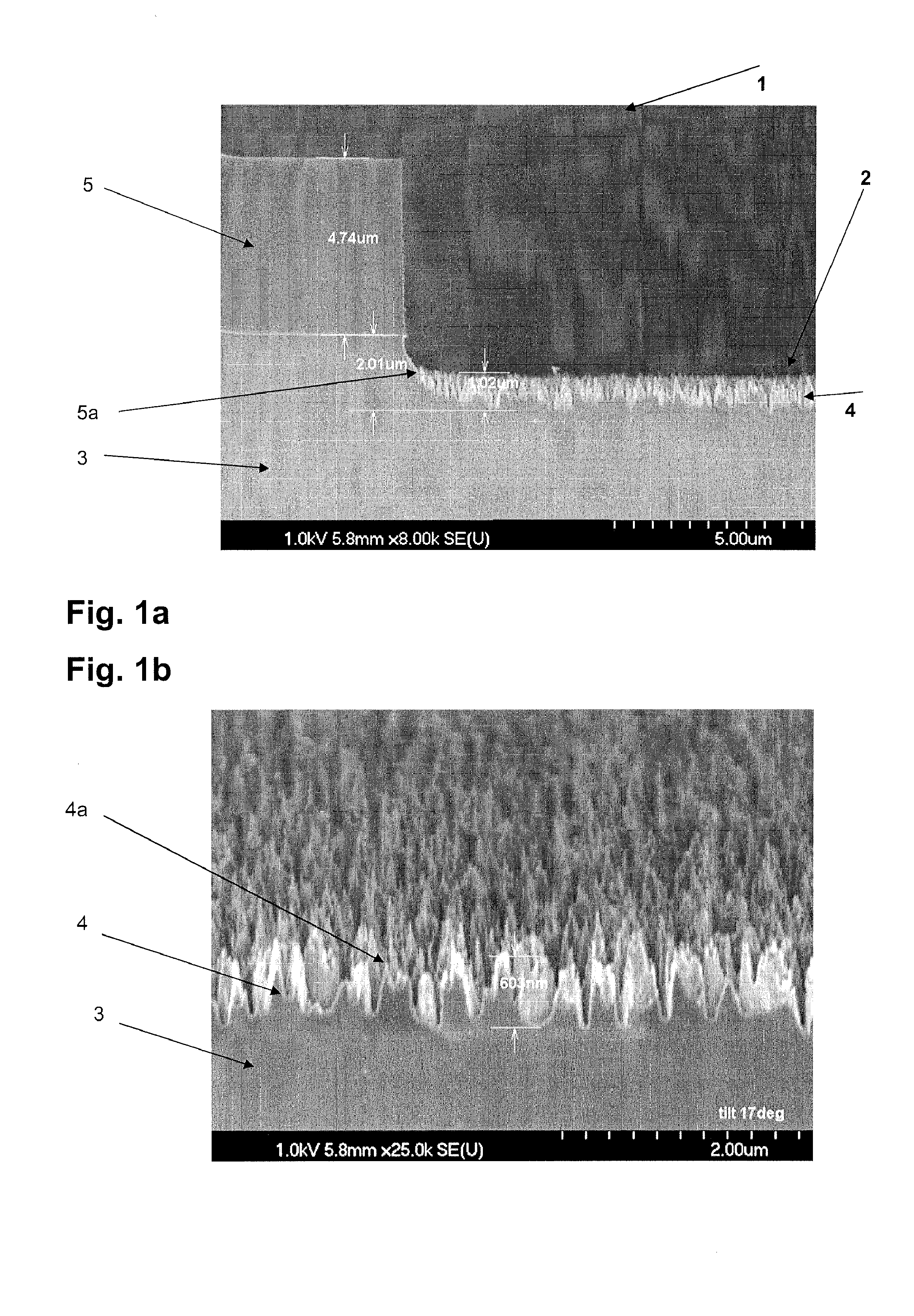
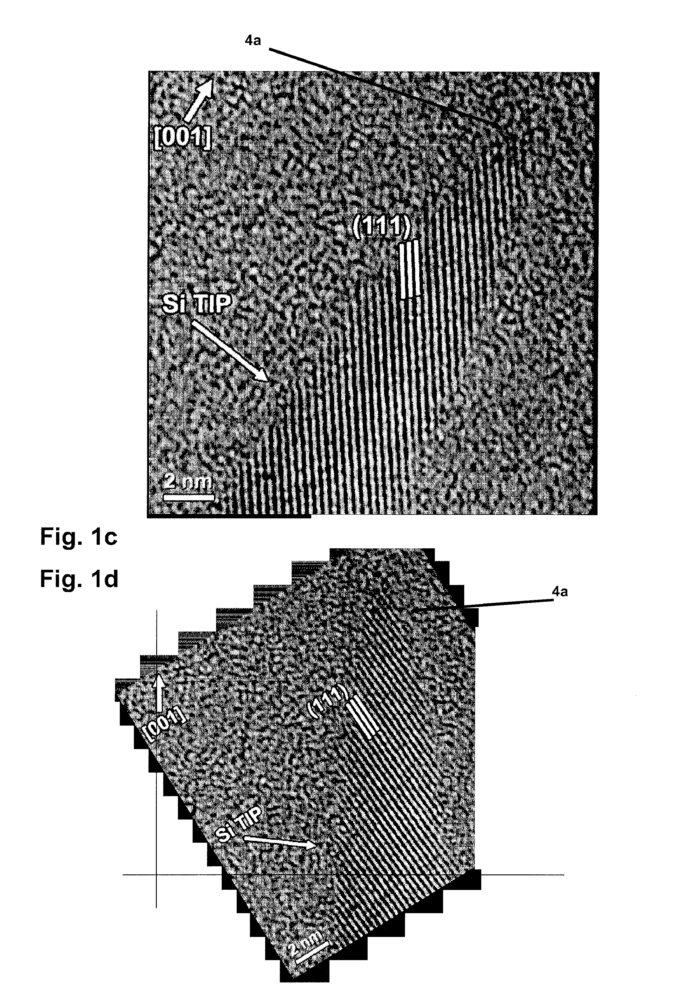
[0114]With reference to FIG. 1a to 1c first an exemplary nanostructure and an illustrative process for forming the same will be described. Similar processes and nanostructures may also be applied in other applications, such as photo electric devices, sensor devices in the form of optical layer structures in optical apparatus, as optical windows and the like, as is already described above and as will be described in the subsequent embodiments. Furthermore, the nanostructures, as are for instance produced by the subsequently described method, may be subjected to further treatments for applying protective layers, modifying the surface and the like.

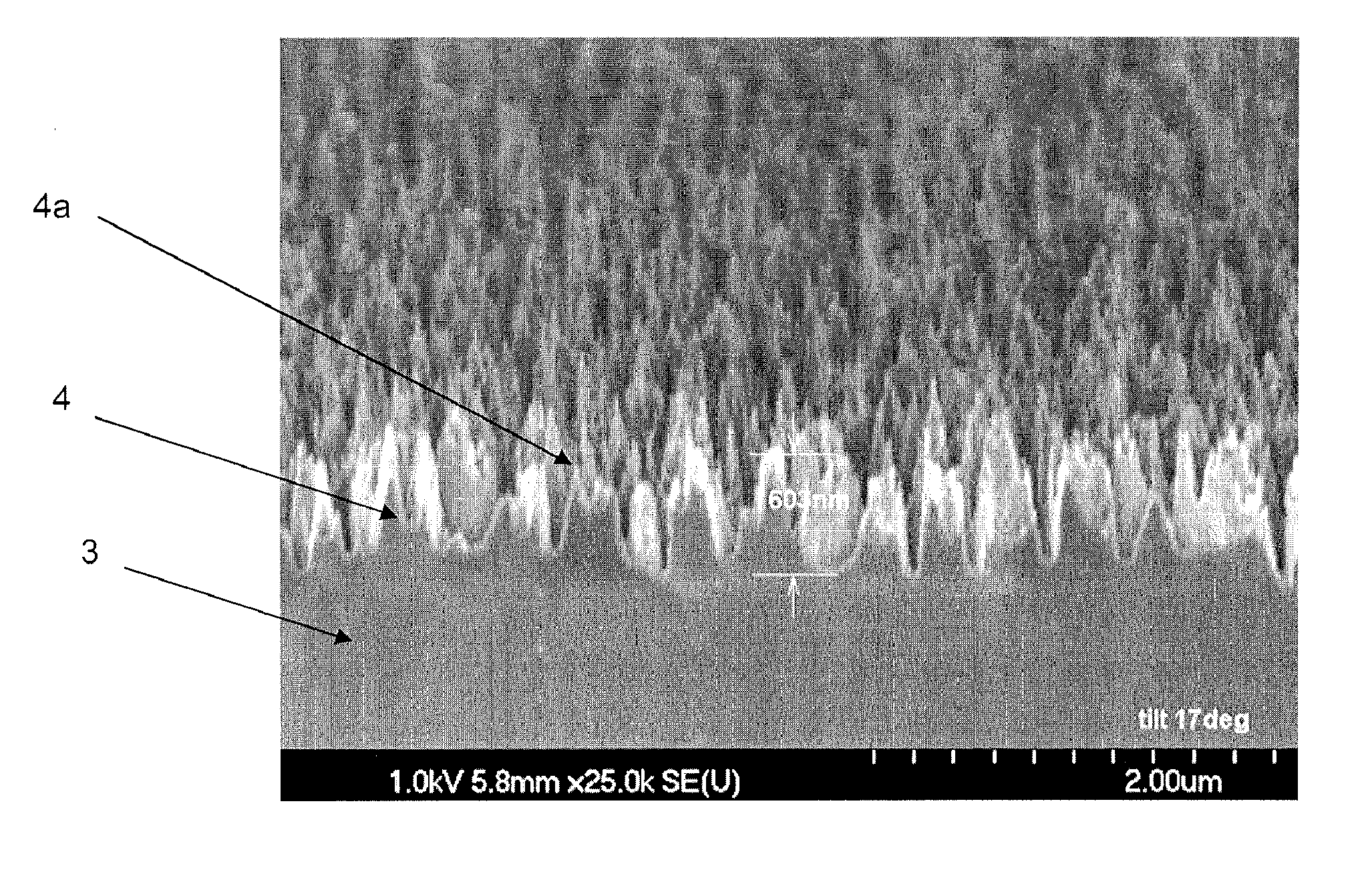
[0115]FIG. 1a illustrates a silicon-containing device 1 comprising a nanostructure 2 that includes a single crystalline silicon base layer 3, on which pin-type silicon structures or elements 4 are formed, which are alternatively (but synonymously) also referred to as structural elements of the nanostructure 2. In this application pin-type sil...


PUM

PropertyMeasurementUnit
heightaaaaaaaaaa
heightaaaaaaaaaa
heightaaaaaaaaaa

Abstract

The invention relates to methods and devices comprising a nanostructure (2;4,4a) for improving the optical behavior of components and apparatuses and/or improving the behavior of sensors by increasing the active surface area. The nanostructure (2) is produced by means of a special RIE etching process, can be modified regarding the composition of the materials thereof, and can be provided with adequate coatings. The amount of material used for the base layer (3) can be reduced by supplying a buffer layer (406). Many applications are disclosed.

Description

FIELD OF THE INVENTION(S)[0001]Generally, the invention relates to the fabrication of structured or patterned surfaces and in particular relates to the production of pin type structures having nano dimensions in the range of for instance below the wavelength of visible light, wherein hereinafter these structures are referred to as nanostructures. The possibilities and technical applications of these structures are emphasized herein.RELATED ART[0002]Many electronic, opto-electronic, sensor and micromechanical devices comprise silicon as one component in doped and / or non-doped, crystalline and / or polycrystalline and / or amorphous form. In order to meet the device specific requirements silicon has usually to be processed in an appropriate manner, which frequently involves the patterning of the silicon.[0003]For the patterning of silicon generally a mask made of photoresist is produced, with the aid of which material removal is controlled during an etch process. In order to produce small...

Claims


Application Information

Patent Timeline
Patent Type & Authority Applications(United States)
IPC IPC(8): H01L31/14H01L31/0232H01L31/0216H01L31/0236H01L21/02H01L31/18H01L21/3065
CPCB81C1/00111B82Y20/00Y02E10/50H01L31/0236H01L31/18B82Y30/00H01L31/02363
Inventor GAEBLER, DANIELBACH, KONRAD
Owner X FAB SEMICON FOUNDRIES
Why Eureka
Try Eureka