
Method of fabricating flexible display device

a display device and flexible technology, applied in the field of display devices, can solve the problems of display panels, tft on plastic substrates instead of glass substrates in the existing panel fabrication process, and can be overly brittle and prone to cracking, etc., and achieve the effect of improving the processing efficiency and reducing the cost of production

Active Publication Date: 2009-10-29
SAMSUNG DISPLAY CO LTD
View PDF3 Cites 96 Cited by
  • Summary
  • Abstract
  • Description
  • Claims
  • Application Information

AI Technical Summary

Benefits of technology

The invention provides a method for making a flexible display device without using a separate separation layer between the plastic substrate and the carrier substrate. Instead, a barrier layer previously formed on the plastic substrate is used to separate the carriers. This method involves applying a transparent adhesive layer on the carrier substrate, laminating a flexible substrate with a barrier layer on top, and then forming a thin film transistor array on the flexible substrate. The method can also involve applying a second transparent adhesive layer on a second carrier substrate, laminating a flexible substrate with a barrier layer on top, and then forming a color filter array on the second flexible substrate. The two flexible substrates are then separated by irradiating a laser beam onto the barrier layer. The technical effect of this method is that it simplifies the fabrication process of flexible display devices and reduces the cost of production.

Problems solved by technology

Conventional LCDs, PDPs, and OLEDs use a glass substrate that can be overly brittle and prone to cracking.
However, fabricating a display panel by directly forming a TFT on the plastic substrate instead of the glass substrate in an existing panel fabrication process still has difficulties in terms of processing due to the flexibility of the plastic substrate.
However, an additional process is needed for forming the separation layer on the carrier substrate, thereby adding process time and expense.

Method used


Image

  • Method of fabricating flexible display device
  • Method of fabricating flexible display device
  • Method of fabricating flexible display device

Examples


Embodiment Construction

[0017]Hereinafter, exemplary embodiments are described in detail with reference to FIGS. 1 to 4F.

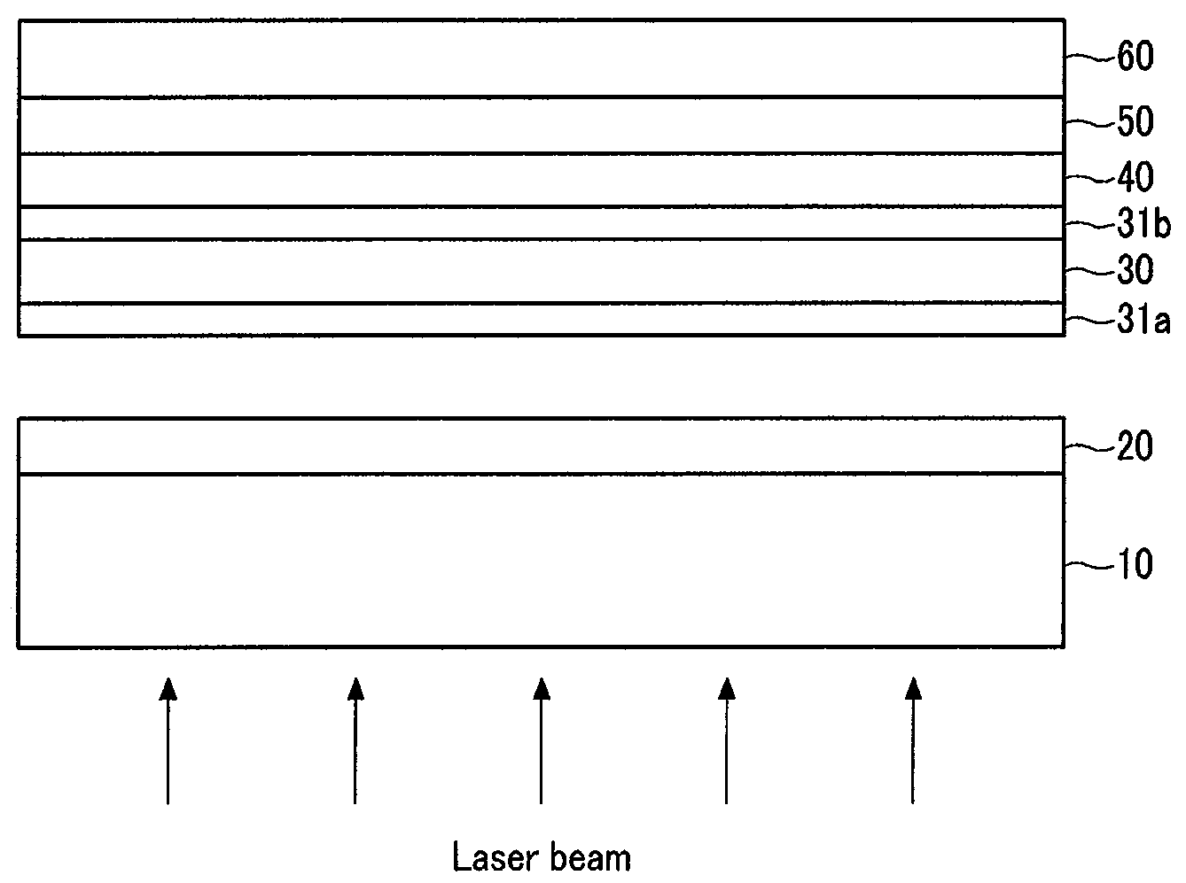
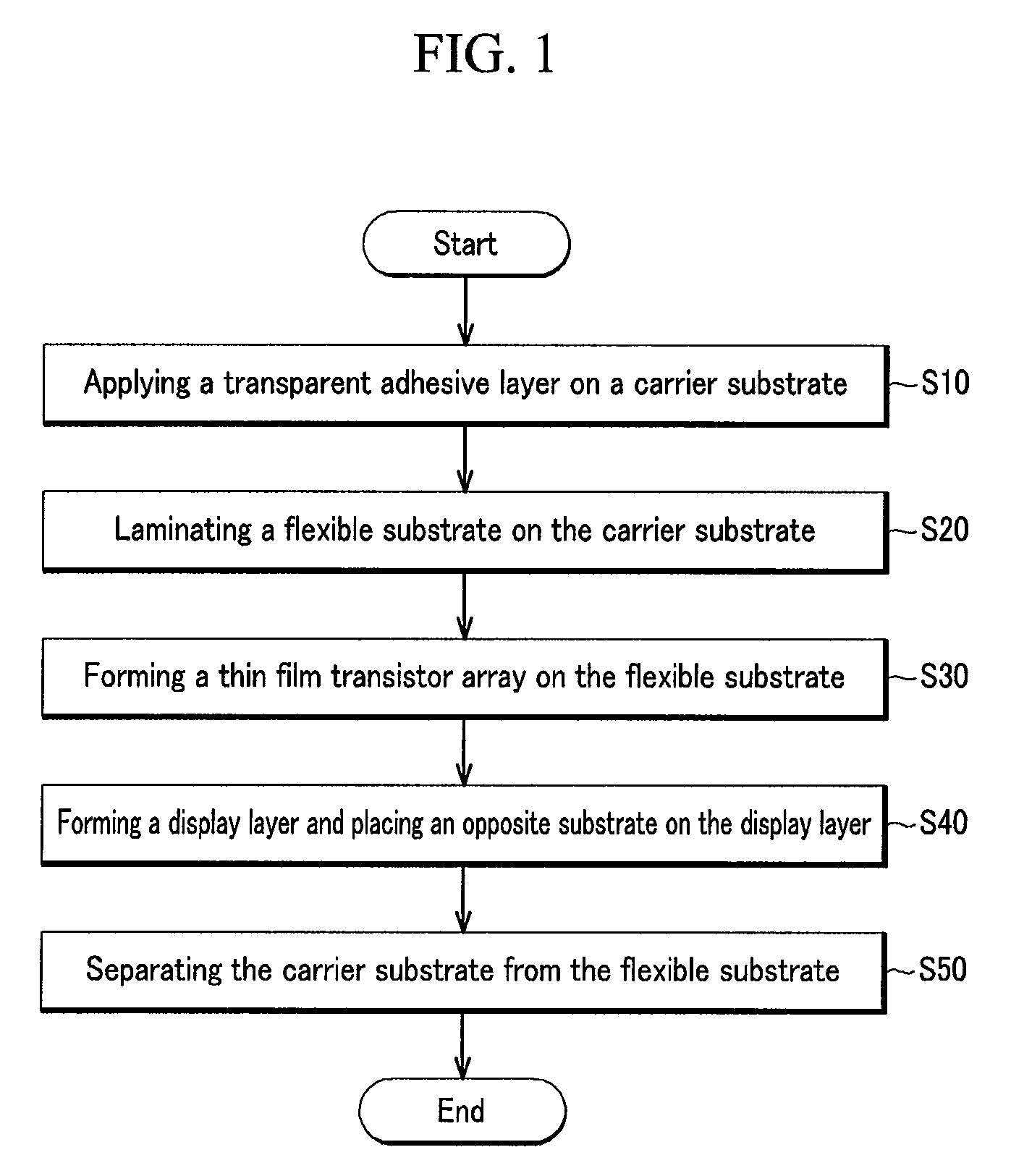
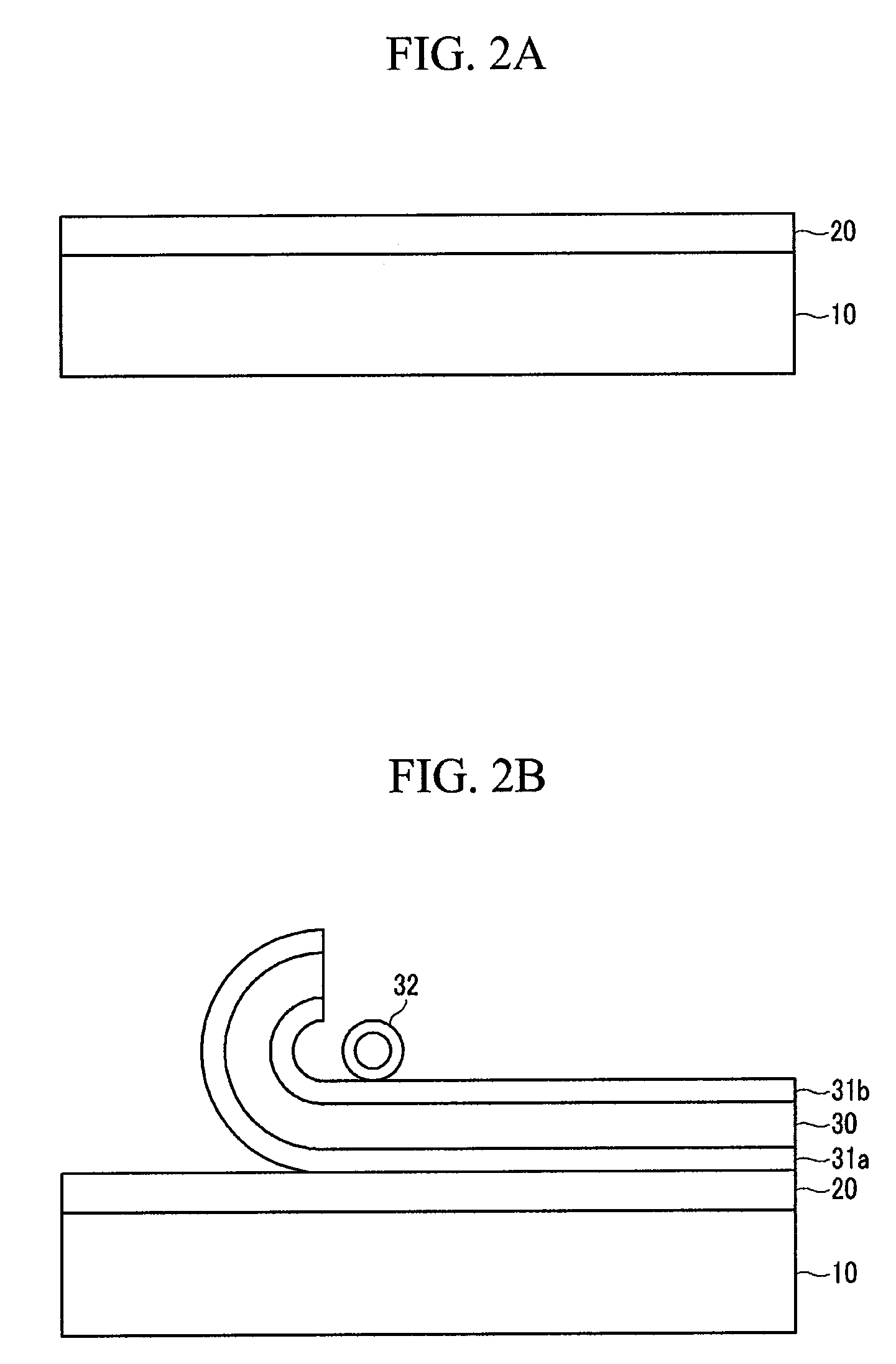
[0018]FIG. 1 is a flow chart showing a process of fabricating a flexible display device in accordance with an embodiment of the present invention. FIGS. 2A-2F are cross-sectional views further illustrating the process of FIG. 1.

[0019]Referring to FIG. 1, a fabricating method of a flexible display device includes applying a transparent adhesive layer on a carrier substrate (step S10), laminating a flexible substrate on the carrier substrate (step S20), forming a thin film transistor (“TFT”) array on the flexible substrate (step S30), forming a display layer and placing an opposite substrate on the display layer (step S40), and separating the carrier substrate from the flexible substrate (step S50). This method is described below in further detail with reference to FIGS. 2A to 2F.

[0020]Referring to FIG. 2A, a transparent adhesive layer 20 is formed on a carrier substrate 10. The carrier su...


PUM

PropertyMeasurementUnit
wavelengthaaaaaaaaaa
glass transition temperatureaaaaaaaaaa
transparentaaaaaaaaaa

Abstract

A method of fabricating a flexible display device, the method including applying a transparent adhesive layer on a carrier substrate, laminating a flexible substrate comprising a barrier layer on the transparent adhesive layer, forming a thin film transistor array on the flexible substrate, and separating the carrier substrate from the flexible substrate by irradiating a laser beam onto the barrier layer.

Description

CROSS-REFERENCE TO RELATED APPLICATION [0001]This application claims priority under 35 U.S.C. §119 to Korean Patent Application No. 10-2008-0040006, filed on Apr. 29, 2008, in the Korean Intellectual Property Office (KIPO), the contents of which are incorporated herein by reference in their entirety.BACKGROUND OF THE INVENTION[0002]1. Field of the Invention[0003]The disclosure relates to display devices, and more particularly, to a method of fabricating a flexible display device.[0004]2. Description of the Related Art[0005]Display devices have recently included flat panel display devices capable of achieving a large display area, lightness and slimness. Flat panel display devices include liquid crystal displays (“LCDs”), plasma display panels (“PDPs”), organic light emitting displays (“OLEDs”), and the like. Conventional LCDs, PDPs, and OLEDs use a glass substrate that can be overly brittle and prone to cracking.[0006]Recently, flexible display devices using a flexible substrate suc...

Claims


Application Information

Patent Timeline
Patent Type & Authority Applications(United States)
IPC IPC(8): G02F1/1333
CPCG02F1/133305H01L29/78603H01L27/1266H01L27/1214H01L27/1218G02F1/13G02F1/1333G02F1/136
Inventor KIM, MYUNG-HWANROH, NAM-SEOKKIM, SANG-IL
Owner SAMSUNG DISPLAY CO LTD
Learn More