Semiconductor light emitting element and method for manufacturing the same

a technology of semiconductors, applied in the direction of semiconductor/solid-state device manufacturing, semiconductor devices, electrical equipment, etc., can solve the problems of poor crystallinity, inability to manufacture zno-based semiconductor light emitting elements including rectangularly divided sapphire a-plane substrates, and inability to grow zno crystals with streak-like projections on their surface, etc., to achieve easy and reliable manufacturing

Inactive Publication Date: 2009-10-29
STANLEY ELECTRIC CO LTD
View PDF2 Cites 7 Cited by
  • Summary
  • Abstract
  • Description
  • Claims
  • Application Information

AI Technical Summary

Benefits of technology

[0035]According to this manufacturing method, a rectangular sapphire A-plane substrate having a thickness of 50 to 500 μm can be easily and reliably manufactured.

Problems solved by technology

When a sapphire C-plane substrate is used, the grown ZnO crystal contains 30° rotated domains, and therefore the crystallinity is poor.
When a sapphire R-plane substrate is used, the grown ZnO crystal has streak-like projections on its surface and is not suitable for device formation.
Therefore when the method disclosed in this patent publication is applied to a sapphire A-plane substrate having a ZnO-based semiconductor layer formed thereon, ZnO-based semiconductor light emitting elements including rectangularly divided sapphire A-plane substrates cannot be manufactured.
In such a test case, the relative depth of the scribed grooves with respect to the thickness of the substrate is smaller than that when the semiconductor light emitting elements are manufactured, and therefore the substrate is more difficult to cleave.
However, the larger the relative thickness of the substrate with respect to the depth of the scribed grooves, i.e., the smaller the relative depth of the scribed grooves, the more difficult to cleave the substrate.

Method used


Image

  • Semiconductor light emitting element and method for manufacturing the same
  • Semiconductor light emitting element and method for manufacturing the same
  • Semiconductor light emitting element and method for manufacturing the same

Examples


Embodiment Construction

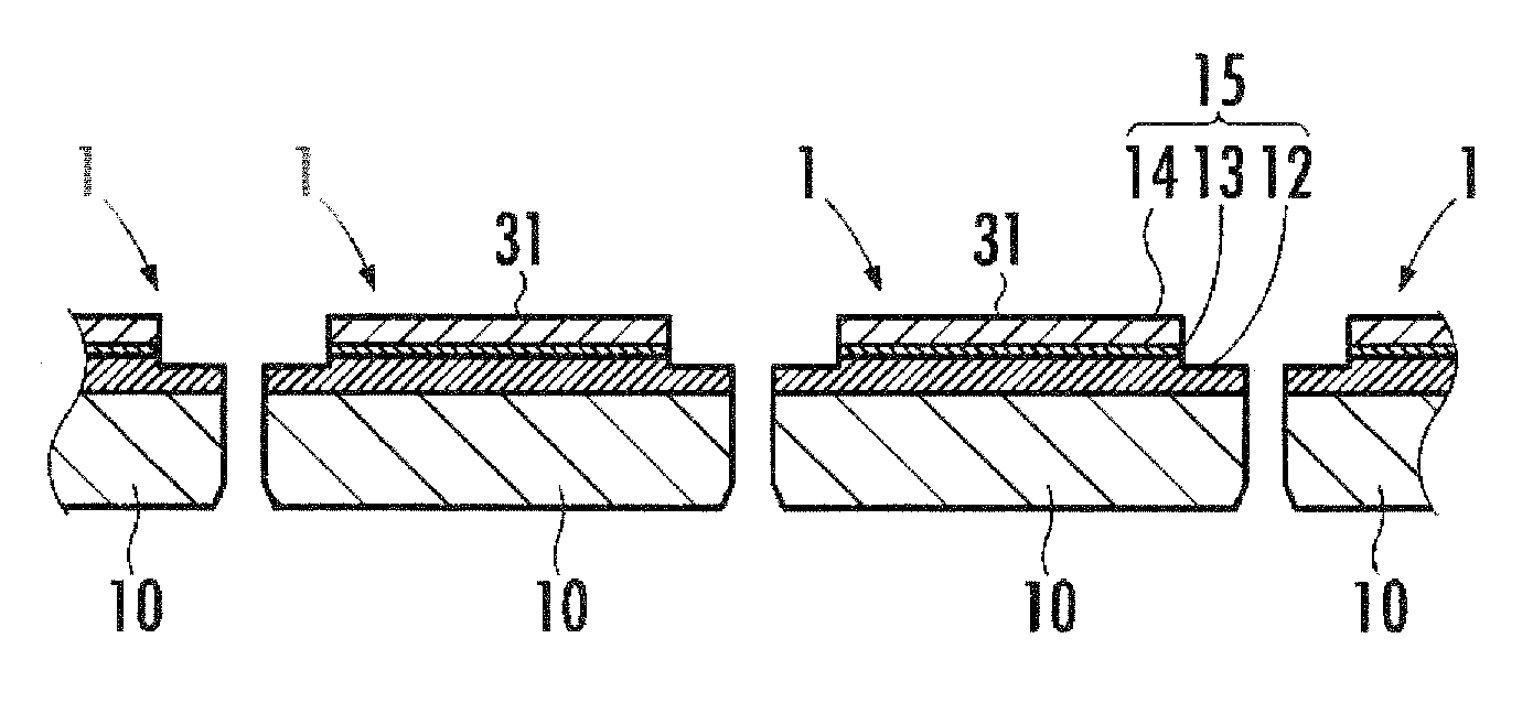
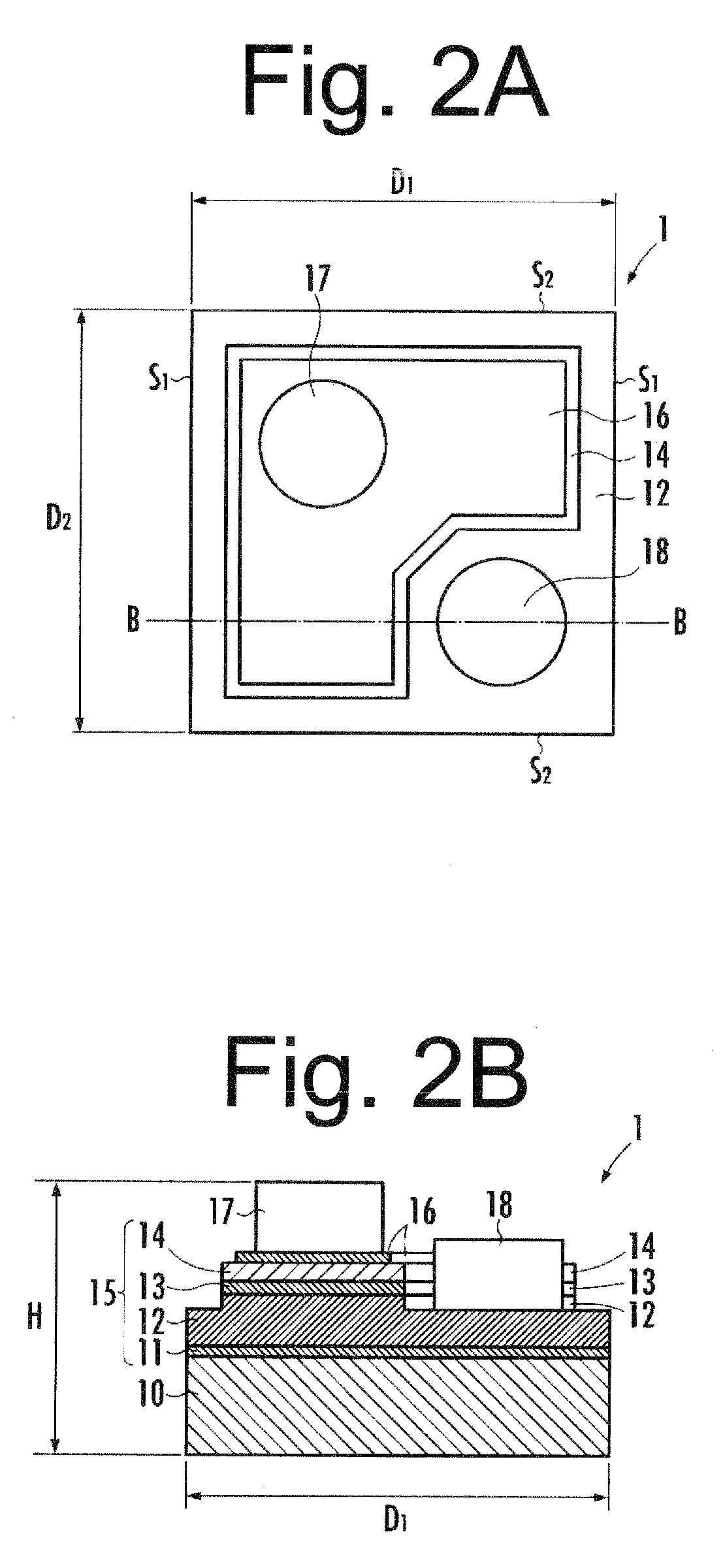
[0042]Next, preferred embodiments of the present invention will be described in more detail with reference to the accompanying drawings. FIG. 2A is a schematic plan view illustrating a ZnO-based semiconductor light emitting element of one embodiment according to the present invention. FIG. 2B is a schematic cross-sectional view taken along line B-B in FIG. 2A. FIG. 3 is a cross-sectional view of an LED lamp using the ZnO-based semiconductor light emitting element shown in FIGS. 2A and 2B. FIGS. 4 and 5A to 5E describe a method for manufacturing the ZnO-based semiconductor light emitting element shown in FIGS. 2A and 2B.

[0043]The ZnO-based semiconductor light emitting element 1 (hereinafter simply referred to as a semiconductor light emitting element) of the present embodiment shown in FIGS. 2A and 2B can include a ZnO-based semiconductor layer serving as an operating layer. The ZnO-based semiconductor layer can be formed on a sapphire A-plane substrate 10 made of an α-sapphire singl...


PUM


Abstract

A ZnO-based semiconductor light emitting element includes a ZnO-based semiconductor layer formed on a rectangular sapphire A-plane substrate having a principal surface lying in the A-plane {11-20}. The substrate has a thickness of 50 to 200 μm and is surrounded by two parallel first side edges forming an angle in a range of 52.7° to 54.7° with respect to the m-axis orthogonal to the c-axis and two parallel second side edges orthogonal to the first side edges. The light emitting element is obtained by: forming, on a surface of the sapphire A-plane substrate opposite to the surface on which the ZnO-based semiconductor layer is formed, first scribed grooves forming an angle in a range of 52.7° to 54.7° with respect to the m-axis and second scribed grooves orthogonal to the first scribed grooves; and breaking the substrate along the first scribed grooves and then along the second scribed grooves.

Description

[0001]This application claims the priority benefit under 35 U.S.C. §119 of Japanese Patent Application No. 2008-114399 filed on Apr. 24, 2008, which is hereby incorporated in its entirety by reference.BACKGROUND OF THE INVENTION[0002]1. Field of the Invention[0003]The present invention relates to a ZnO-based semiconductor light emitting element and to a method for manufacturing the same.[0004]2. Description of the Related Art[0005]ZnO-based semiconductor light emitting elements have advantages over other semiconductor light emitting elements, such as having a larger exciton binding energy, using lower-cost raw materials, and being less harmful to people and the environment. Therefore, such ZnO-based semiconductor light emitting elements are expected to provide high-efficiency and low-power consumption devices.[0006]Examples of the substrates used in ZnO-based semiconductor light emitting elements include zinc oxide (ZnO) substrates, sapphire (α-Al2O3) substrates, and silicon carbide...

Claims


Application Information

Patent Timeline
Patent Type & Authority Applications(United States)
IPC IPC(8): H01L33/00H01L21/304H01L33/06H01L33/16H01L33/28H01L33/36H01L33/56H01L33/62
CPCH01L33/16H01L33/28H01L2224/45144H01L2224/48091H01L2224/48257H01L2924/00014H01L2924/00
Inventor HORIO, NAOCHIKA
Owner STANLEY ELECTRIC CO LTD
Why Eureka
Try Eureka