Liquid crystal display device

a liquid crystal display and display device technology, applied in semiconductor devices, optics, instruments, etc., can solve the problems of reliability depending on the relationship between ito and view angle characteristics, and achieve the effect of maintaining sealing reliability and eliminating blanking

Active Publication Date: 2009-10-29
JAPAN DISPLAY INC +1
View PDF2 Cites 90 Cited by
  • Summary
  • Abstract
  • Description
  • Claims
  • Application Information

AI Technical Summary

Benefits of technology

[0012]The present invention intends to eliminate blanking due to the effect of scanning in the display region

Problems solved by technology

On the other hand, view angle characteristics become a problem in the liquid crystal display devices.
In a case of covering the scanning line lead with ITO, close adhesion between ITO and a sealant causes a problem.
However, in a case where the sealant is in direct contact with the conductive film such as an IT

Method used


Image

  • Liquid crystal display device
  • Liquid crystal display device
  • Liquid crystal display device

Examples


embodiment 1

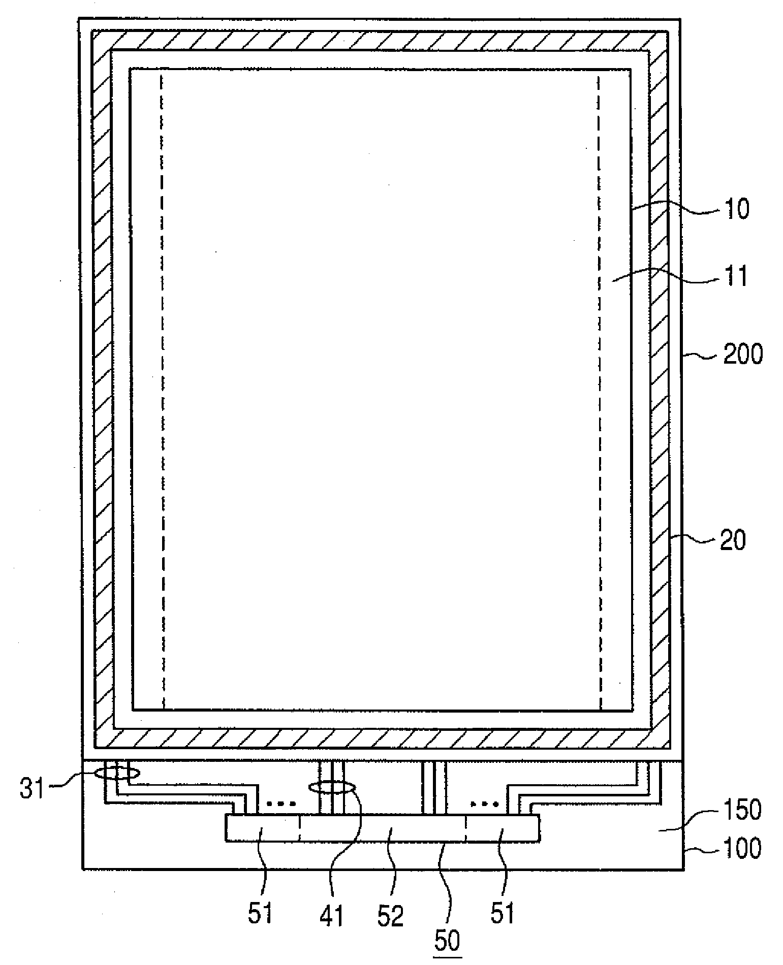
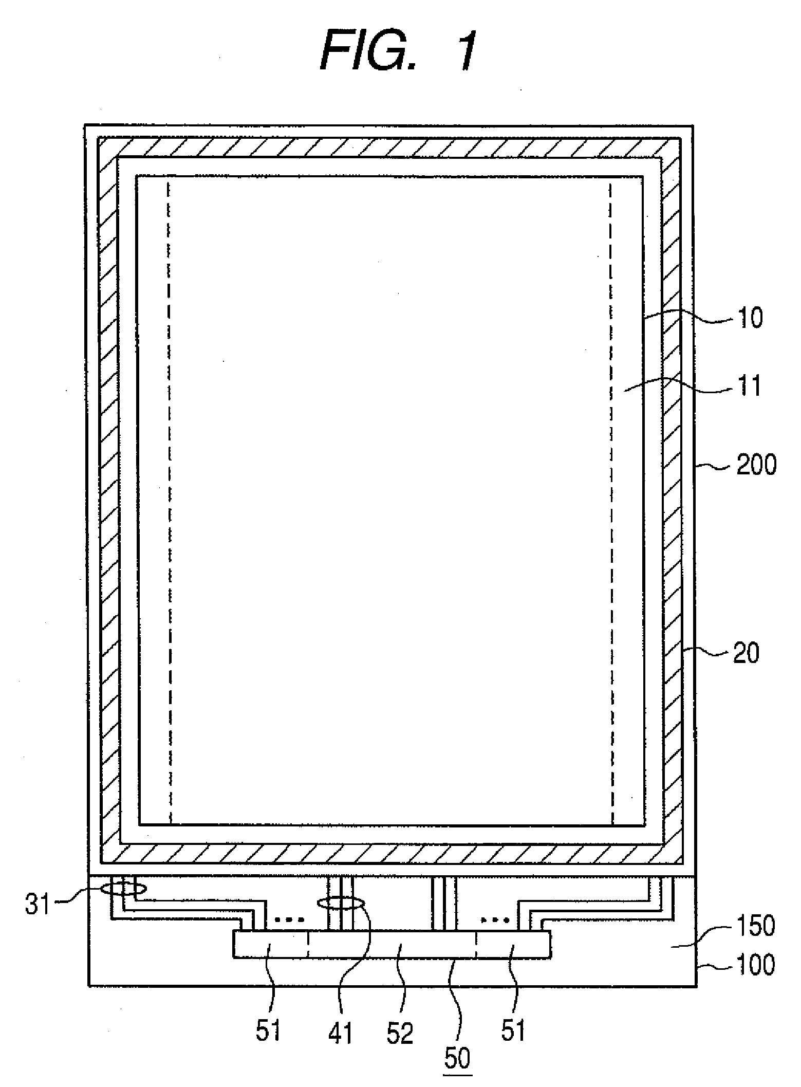
[0040]FIG. 1 is a plan view of a liquid crystal display device applied with the present invention which is used, for example, in cellular phones. In FIG. 1, a counter substrate 200 is disposed above a TFT substrate 100. A liquid crystal layer is put between the TFT substrate 100 and the counter substrate 200. The TFT substrate 100 and the counter substrate 200 are bonded by a sealant 20 formed to a frame portion. The TFT substrate 100 is made larger than the counter substrate 200, in which a terminal portion 150 for supplying a power source, video signals, scanning signals, etc. to the TFT substrate 100 is formed to a portion of the TFT substrate which is made larger than the counter substrate 200.

[0041]Further, an IC driver 50 for driving scanning lines, video signal lines, etc. are disposed to the terminal portion 150. The IC driver 50 is divided into three regions in which a video signal driving circuit 52 is disposed at a central portion and scanning signal driving circuits 51 a...

embodiment 2

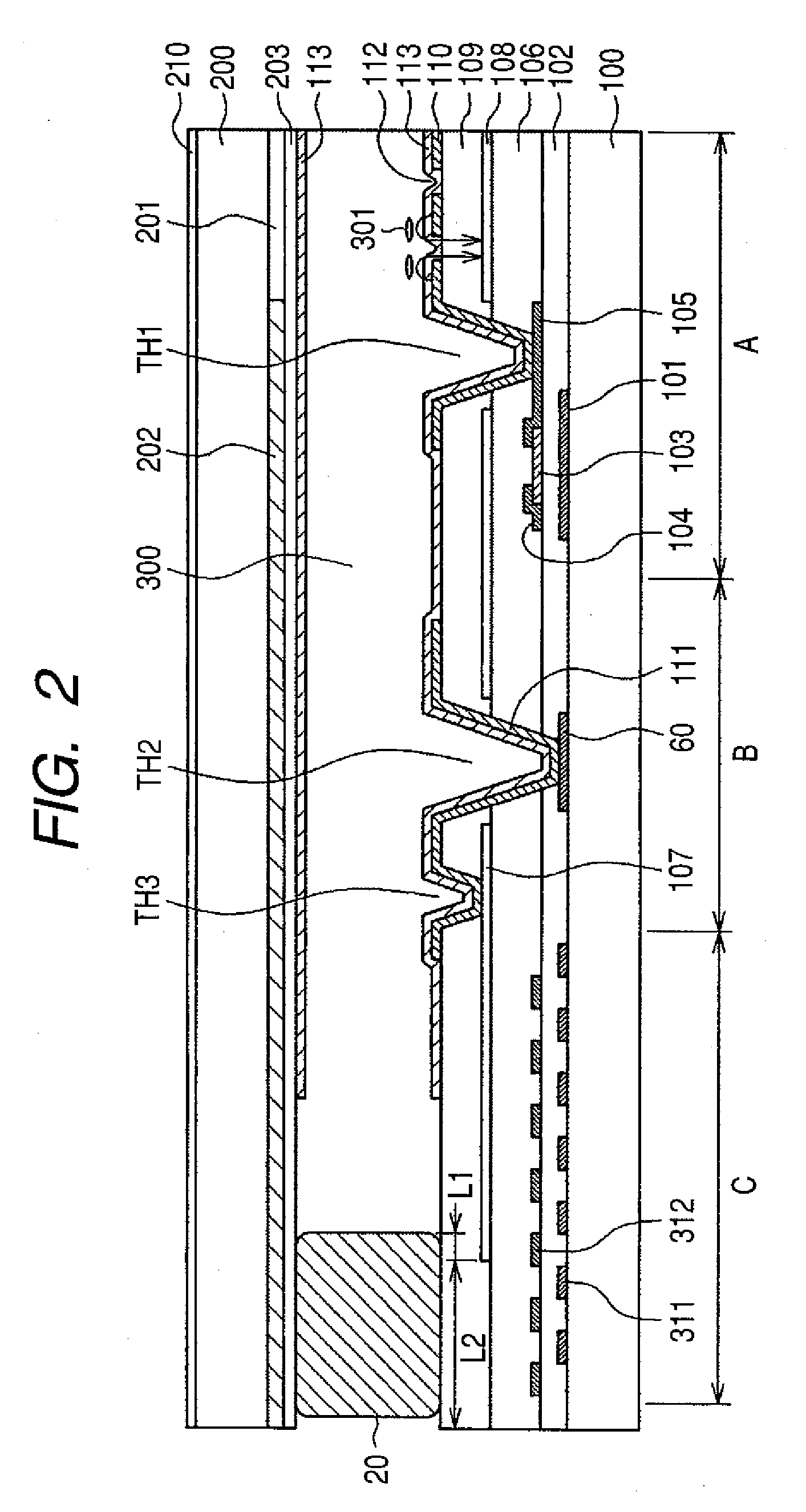
[0076]In the liquid crystal display device of the IPS system of Embodiment 1, the planar common electrode 108 is formed above the inorganic passivation film 106, the upper insulative film 109 is formed thereabove, and the interdigitated pixel electrode 110 is formed further thereabove. Contrary to the arrangement of the electrodes in the liquid crystal display device of Embodiment 1, a planar pixel electrode 110 may be formed on the inorganic passivation film 106 and an interdigitated common electrode 108 may be formed thereabove while sandwiching the upper insulative film 109 between them. The shape of the common electrode 108 in this case may be identical with that for the interdigitated electrode shown in FIG. 3.

[0077]In FIG. 7, a planar pixel electrode 110 is formed above the inorganic passivation film 106 in the pixel area. An upper insulative film 109 is formed above the planar pixel electrode 110, and an interdigitated common electrode 108 is formed above the upper insulative...


PUM


Abstract

An IPS type liquid crystal display device capable of preventing a blanking phenomenon generated to the periphery of a screen caused by charging at the inside of a counter substrate due to the effect of a gate voltage applied to scanning line leads. In a pixel area A constituting a display region, a pixel electrode is disposed by way of an insulative film above a common electrode formed in a planar shape. In a scanning line lead area, the scanning line leads have first scanning line leads and second scanning lines formed in different layers for decreasing the width of the scanning line lead area. The scanning line leads are covered with a shield electrode formed coplanar with the common electrode. Since the shield electrode is extended as far as a portion below a sealant, the shielding effect is enhanced. Further, since the insulative film is present between the sealant and the shield electrode, the sealing effect is not deteriorated.

Description

CLAIM OF PRIORITY[0001]The present application claims priority from Japanese Patent Application JP 2008-116981 filed on Apr. 28, 2008, the content of which is hereby incorporated by reference into this application.BACKGROUND OF THE INVENTION[0002]1. Field of the Invention[0003]The present invention concerns a display device and, particularly, it relates to a liquid crystal display device of an in-plane electric field system (IPS) excellent in view angle characteristics with no image unevenness also at the periphery of a display region.[0004]2. Description of Related Art[0005]In a liquid crystal display device, a TFT substrate having pixel electrodes and thin film transistors (TFT) formed in a matrix and a counter substrate opposed to the TFT substrate and having color filters, etc, formed at portions corresponding to the pixel electrode of the TFT substrate are disposed, and liquid crystals are put between the TFT substrate and the counter substrate. Then, images are formed by contr...

Claims


Application Information

Patent Timeline
IPC IPC(8): G02F1/1343
CPCG02F1/134363G02F1/1345G02F1/136209G02F2001/13456G02F1/13306G02F2001/134372G02F1/133512G02F1/1339G02F1/136286G02F2001/136218G02F1/133345G02F1/13456G02F1/134372G02F1/136218G02F1/134336G02F1/13439G02F1/1368G02F1/133514H01L27/124H01L27/1222H01L29/78669
Inventor ANJO, KENJINAGAMI, TAKAHIROHATAKEYAMA, KENICHI
Owner JAPAN DISPLAY INC
Why Eureka
Try Eureka