Method of fabricating phase change memory device

a phase change memory and memory device technology, applied in the direction of semiconductor devices, bulk negative resistance effect devices, electrical appliances, etc., can solve the problems of difficult to reliably fill the hole, reduced phase change film yield, and difficult pre-cleaning of contact holes before film-coating becomes too complicated, etc., to achieve the effect of substantially increasing the fabrication yield

Inactive Publication Date: 2009-10-29
IND TECH RES INST
View PDF2 Cites 6 Cited by
  • Summary
  • Abstract
  • Description
  • Claims
  • Application Information

AI Technical Summary

Benefits of technology

[0008]The present invention provides a phase change memory (PCM) device having reduced heating area.
[0009]The present invention further provides a method of fabricating a small size PCM device, wherein the fabrication yield is substantially increased.
[0010]The present invention still provides a simple method of fabricating a PCM device.
[0017]The present invention employs spacers comprised of phase change material as the contact hole structures of the thermal electrodes so the size of contact area between the phase change material and the thermal electrode in PCM device is smaller than that formed by a photolithography process, and is smaller than that of “surface contact structure”. Moreover, the process of the present invention is simpler than the conventional process. Furthermore, problems caused by the misalignment of the phase change material and the contact holes of the top electrodes can be effectively avoided. In the process provided by the present invention, the difficulty of filling the holes due to the size of the holes being too small, or the difficulty of plasma gas entering into the holes when the top portions of the film on sidewalls are jointed may be effectively avoided. Furthermore, when the planarization of the PC material film is developed successfully, the cross spacer structure of the present invention is not limited to application in the phase change memory, but can also be applied in a 3D-NVM structure.

Problems solved by technology

However, at present, most known techniques relate to complicated method of etching contact holes in the dielectric layer or sacrificial layer for reducing heating area of the phase change film.
When the contact holes are of a nanometer size, it would be difficult to reliably fill the hole and yield of the phase change film would be reduced significantly, and the dry pre-cleaning for the contact holes before film-coating becomes too complicated.

Method used


Image

  • Method of fabricating phase change memory device
  • Method of fabricating phase change memory device
  • Method of fabricating phase change memory device

Examples


Embodiment Construction

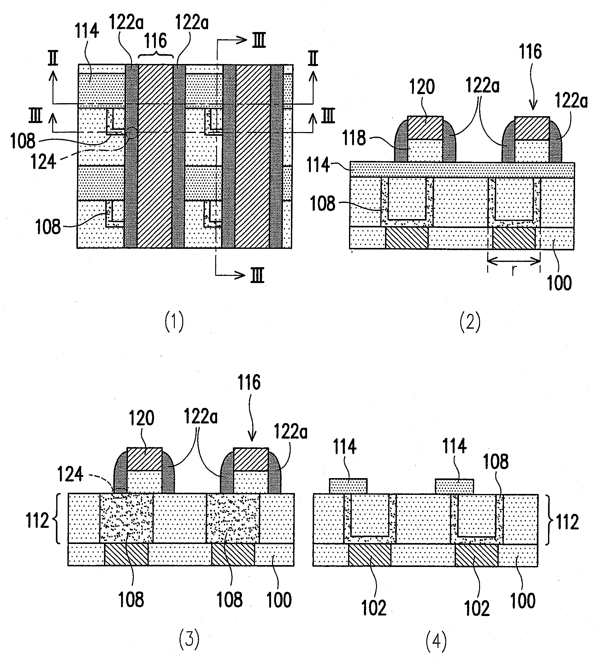
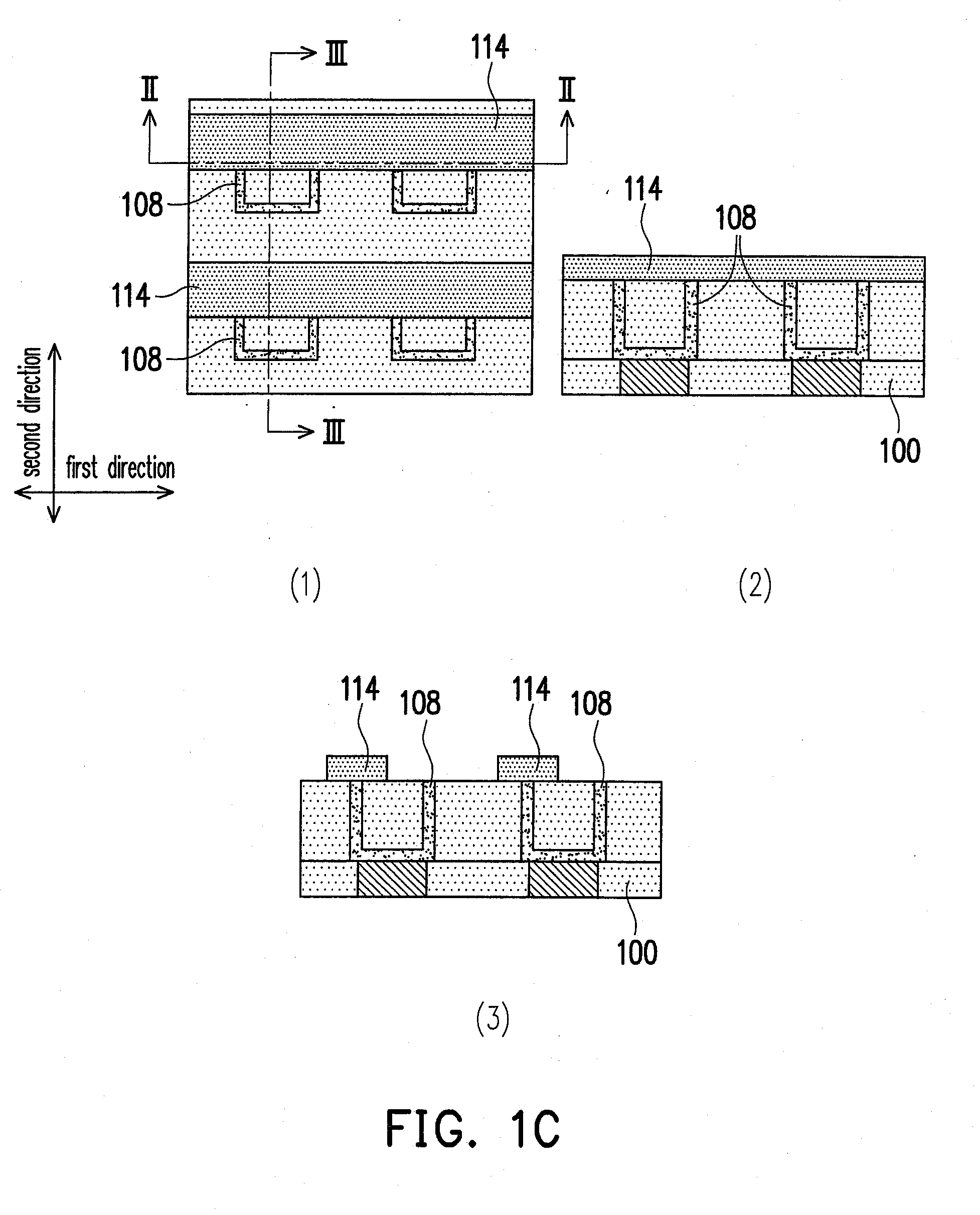
[0023]FIGS. 1A to 1G are views illustrating the process steps of fabricating a phase change memory (PCM) device according to a preferred embodiment of the present invention.

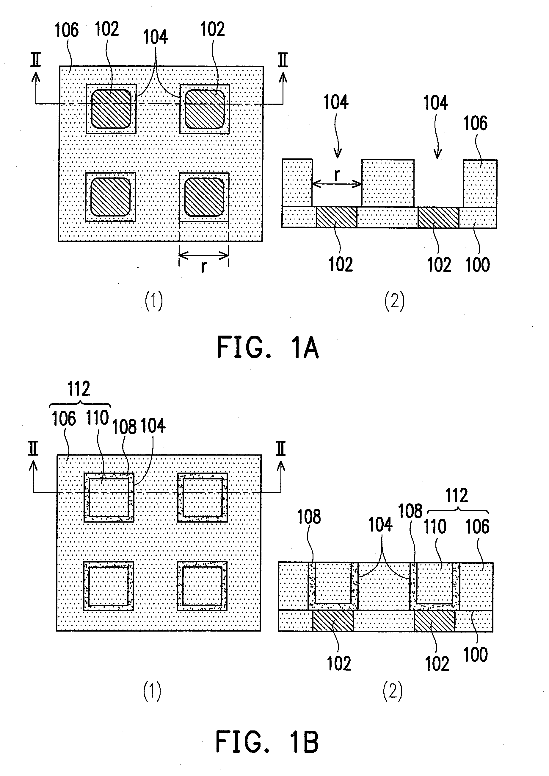
[0024]Referring to FIG. 1A, Part (1) is a top view of the device, and Part (2) is a sectional view along line II-II of Part (1). First, a substrate 100 having a plurality of bottom electrodes 102 formed therein is provided. Next, a first dielectric layer 112 is disposed over the substrate, for example, having a first oxide layer 106 comprising a plurality of openings 104 formed therein, wherein the openings 104 exposes the bottom electrodes 102. The aperture r of each opening 104 corresponds to the thickness of the subsequently formed PC material spacers, which will be described in detail later.

[0025]Referring to FIG. 1B, Part (1) is a top view of the device, and Part (2) is a sectional view along the line II-II of Part (1). A thermal electrode material is formed over the substrate 100, wherein the thermal electr...


PUM

PropertyMeasurementUnit
thicknessaaaaaaaaaa
thicknessaaaaaaaaaa
thicknessaaaaaaaaaa

Abstract

In a method of fabricating a phase change memory (PCM) device, a substrate having bottom electrodes formed therein is provided. A first dielectric layer having cup-shaped thermal electrodes is formed over the substrate. Second dielectric layers are formed on the substrate. Stacked structures are formed on the substrate. A PC material film is formed over the substrate and covers the stacked structures and the second dielectric layers. The PC material film is anisotropically etched to form PC material spacers on sidewalls of the stacked structures, and each of the PC material spacers physically and electrically contacts each of the cup-shaped thermal electrodes and top electrodes. The PC material spacers include phase change material. The PC material spacers are over-etched to remove the PC material film on the sidewalls of the second dielectric layers.

Description

CROSS-REFERENCE TO RELATED APPLICATION[0001]This application is a divisional of and claims priority benefit of an application Ser. No. 11 / 463,899, filed on Aug. 11, 2006, now pending, which claims the priority benefit of Taiwan application serial no. 94147152, filed on Dec. 29, 2005. The entirety of each of the above-mentioned patent applications is hereby incorporated by reference herein and made a part of this specification.BACKGROUND OF THE INVENTION[0002]1. Field of the Invention[0003]The present invention relates to a semiconductor memory device and method of fabricating the same, and more particularly, to a semiconductor memory device and phase change memory device with a small heating area formed through a simple process, and a method of fabricating the same.[0004]2. Description of Related Art[0005]Along with the rapid development and advanced function requirements of portable products, nowadays a global market demand for memory is expanding rapidly, wherein the fast developm...

Claims


Application Information

Patent Timeline
Patent Type & Authority Applications(United States)
IPC IPC(8): H01L47/00
CPCH01L27/2463H01L45/06H01L45/126H01L45/1691H01L45/124H10B63/80H10N70/8265H10N70/8413H10N70/231H10N70/068
Inventor CHEN, WEI-SU
Owner IND TECH RES INST
Why Eureka
Try Eureka