Method of forming interconnection line and method of manufacturing thin film transistor substrate

Inactive Publication Date: 2009-10-29
SAMSUNG ELECTRONICS CO LTD
View PDF5 Cites 10 Cited by
  • Summary
  • Abstract
  • Description
  • Claims
  • Application Information

AI Technical Summary

Benefits of technology

[0008]Accordingly, one or more embodiments of the present invention may solve the above-mentioned problems occurring in the prior art, and provide a method of forming an interconnection line and a method of manufactur

Problems solved by technology

As the length of the interconnection line is increased, the resistivity and capacitance of the interconnection line are abruptly increased, resulting in image distortion due to an RC delay phenomenon.
Additionally, as the line width of the interconnection line is decreased, the resistance R is increased, resulting in increased leakage current.
In this case, it is required to apply a relatively high supply voltage to the interconnection line, and this causes increase

Method used


Image

  • Method of forming interconnection line and method of manufacturing thin film transistor substrate
  • Method of forming interconnection line and method of manufacturing thin film transistor substrate
  • Method of forming interconnection line and method of manufacturing thin film transistor substrate

Examples


Embodiment Construction

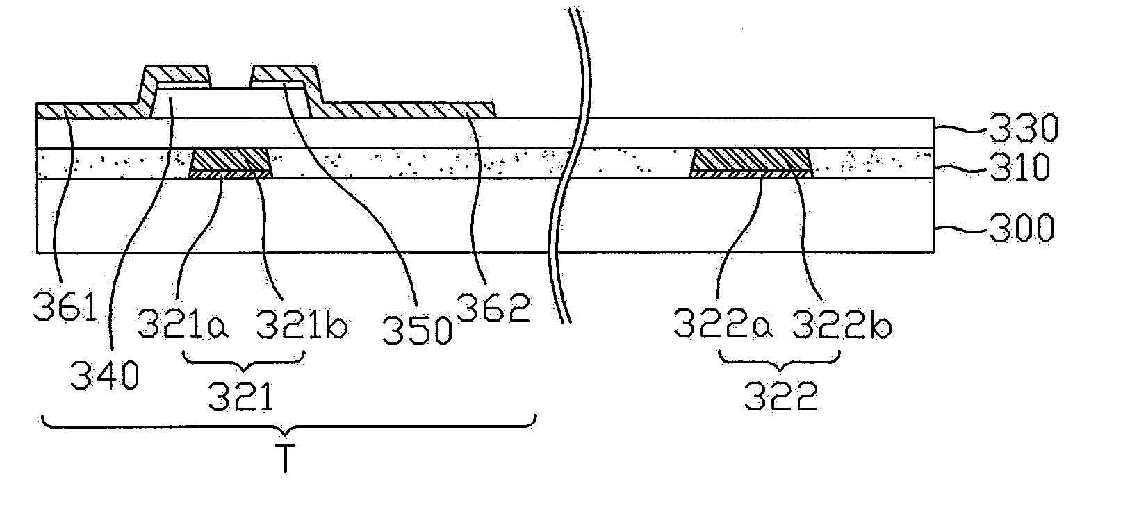
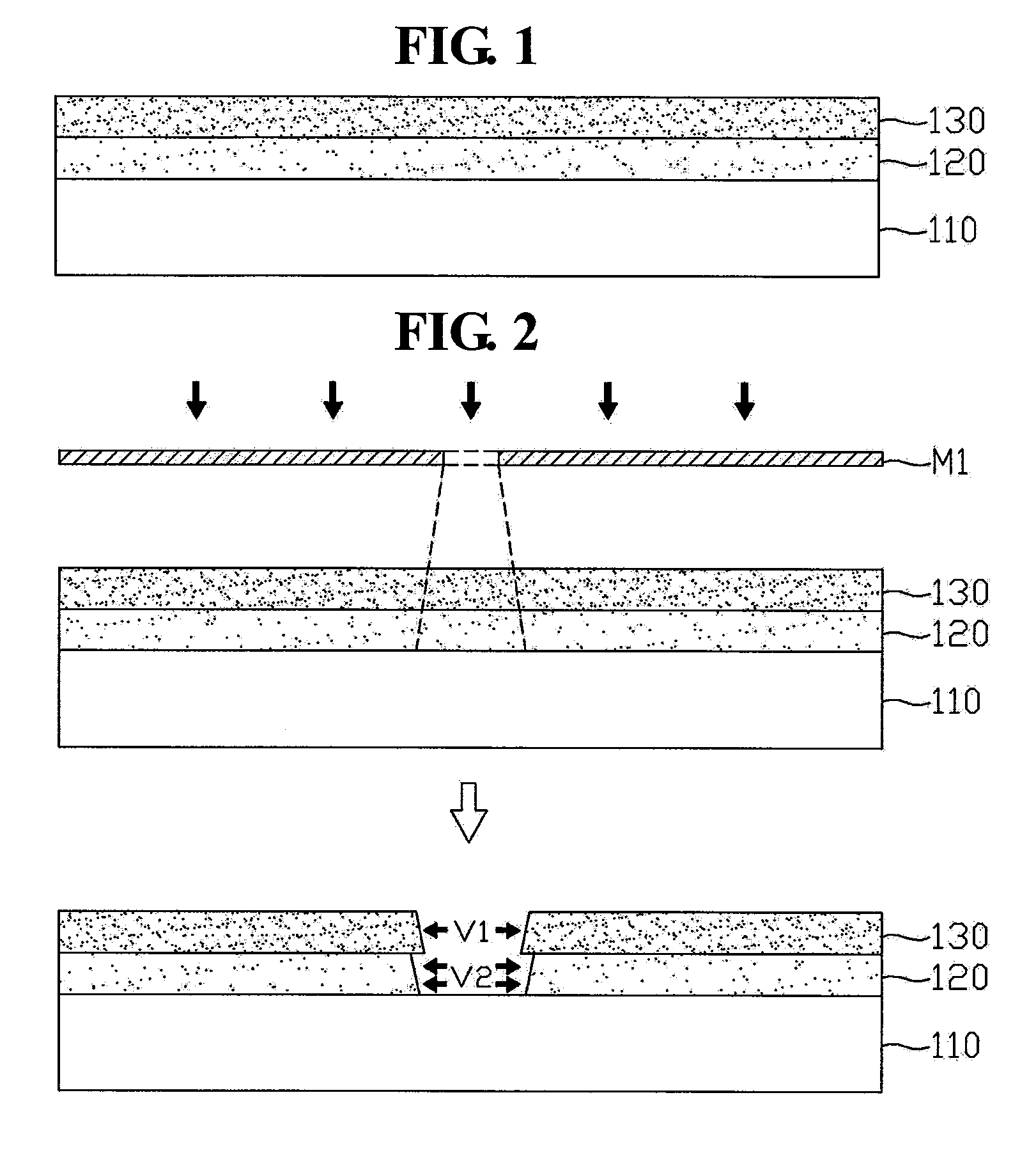
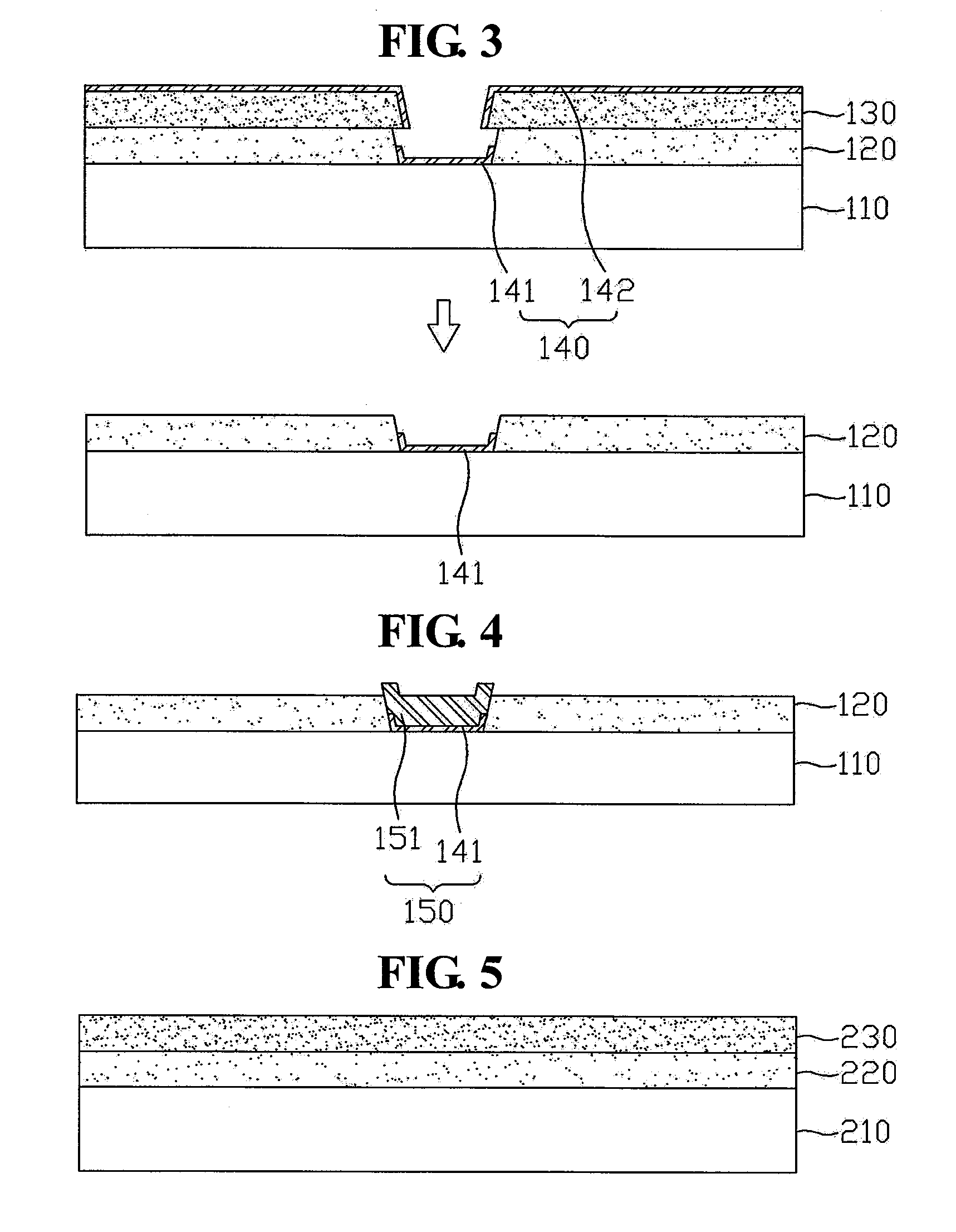
[0039]Hereinafter, one or more embodiments of the present invention will be described in detail with reference to the accompanying drawings. However, the present invention is not limited to the embodiments disclosed hereinafter, but can be embodied in many diverse forms and should not be construed as being limited to the embodiments set forth herein. Rather, these embodiments are provided to assist those of ordinary skill in the art in a comprehensive understanding of the embodiments of the present invention. As such, the present invention is only defined within the scope of the appended claims. In the drawings, sizes and relative sizes of layers and areas may be exaggerated for clarity in explanation.

[0040]It will be understood that when an element or layer is referred as being “on” another element or layer, the element or layer may be located directly on another element or layer, or intervening elements or layers may be present. By contrast, when an element or layer is referred as...


PUM


Abstract

A method of forming an interconnection line and a method of manufacturing a thin film transistor substrate are provided in accordance with one or more embodiments of the present invention. The method of forming an interconnection line in accordance with one or more embodiments of the present invention includes preparing a substrate, forming a lower organic layer and an upper organic layer on the substrate in lamination, forming trenches in parts of the upper organic layer and the lower organic layer, forming a lower interconnection layer in the trenches formed in parts of the lower organic layer, removing the upper organic layer, and filling the trenches formed in parts of the lower organic layer with an upper interconnection layer.

Description

CROSS-REFERENCE TO RELATED APPLICATION[0001]This application claims priority to and the benefit of Korean Patent Application No. 10-2008-0038303 filed on Apr. 24, 2008, in the Korean Intellectual Property Office, the disclosure of which is incorporated herein by reference in its entirety.BACKGROUND[0002]1. Technical Field[0003]One or more embodiments of the present invention generally relate to a method of forming an interconnection line and a method of manufacturing a thin film transistor substrate. More particularly, one or more embodiments of the present invention relate to a method of forming an interconnection line and a method of manufacturing a thin film transistor substrate to achieve a low-resistance characteristic by forming the interconnection line with a sufficient thickness using a trench structure.[0004]2. Description of the Related Art[0005]With the development of mass production and improved technology, deficiencies of liquid crystal display (LCD), such as narrow vie...

Claims


Application Information

Patent Timeline
IPC IPC(8): H01L21/336H01L23/52
CPCH01L21/0272H01L21/76804H01L21/76843H01L27/1248H01L21/76879H01L27/124H01L21/76873H01L27/1214H01L29/42384
Inventor PARK, JEONG-MINLEE, HI-KUKJUNG, DOO-HEE
Owner SAMSUNG ELECTRONICS CO LTD
Why Eureka
Try Eureka