High Voltage LDMOS Transistor and Method

a technology of ldmos transistor and structure, which is applied in the direction of transistors, electrical equipment, semiconductor devices, etc., can solve the problems of mos transistor breakdown, nmos transistor threshold voltage (vt) to undergo undesirable shift to the positive side, etc., and achieve the effect of improving suppression of hot carrier effects

Inactive Publication Date: 2009-11-05
TAIWAN SEMICON MFG CO LTD
View PDF54 Cites 57 Cited by
  • Summary
  • Abstract
  • Description
  • Claims
  • Application Information

AI Technical Summary

Benefits of technology

[0004]These and other problems are generally solved or circumvented, and technical advantages are generally achieved, by preferred embodiments of the present invention which provide an LDMOS transistor comprising a gate electrode extended on an upper boundary of a dielectric region that separates the gate electrode from the drain region of the LDMOS transistor. Moreover, at an area close to an edge of the extended portion, the gate electrode further projects downwards into a convex-shaped recess or groove in the upper boundary of the dielectric region, forming a tongue. LDMOS transistors with this structure may provide improved suppression of hot carrier effects.

Problems solved by technology

Electric breakdown in MOS transistors is a well recognized problem.
This so-called hot carrier effect may cause various problems in a MOS transistor.
The trapped electrons may cause the threshold voltage (Vt) of an NMOS transistor to undergo an undesirable shift to the positive side.
The hot carrier effect may also lead to long term device degradation and reduced reliability.
Under extreme circumstances, snapback breakdown may even cause permanent physical damage in the gate oxide.

Method used


Image

  • High Voltage LDMOS Transistor and Method
  • High Voltage LDMOS Transistor and Method
  • High Voltage LDMOS Transistor and Method

Examples


Embodiment Construction

[0016]The making and using of the presently preferred embodiments are discussed in detail below. It should be appreciated, however, that the present invention provides many applicable inventive concepts that can be embodied in a wide variety of specific contexts. The specific embodiments discussed are merely illustrative of specific ways to make and use the invention, and do not limit the scope of the invention.

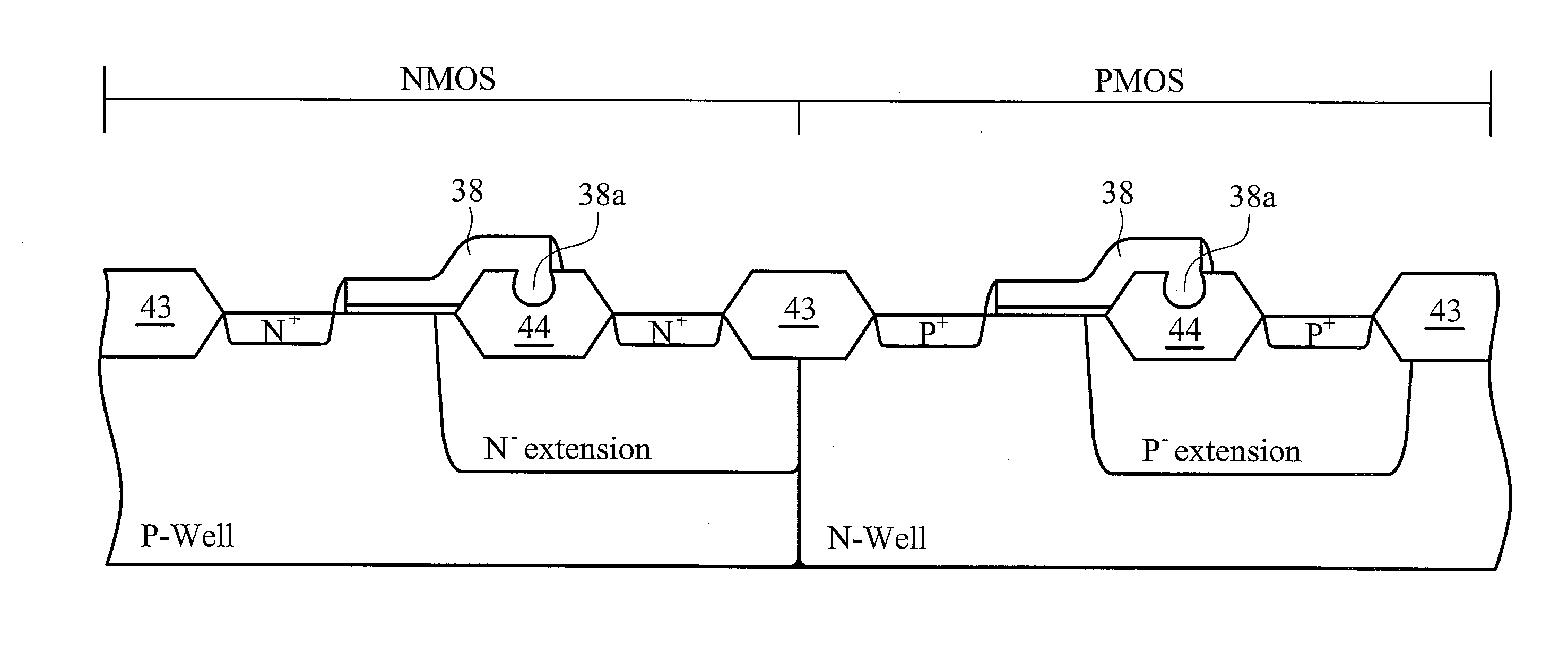
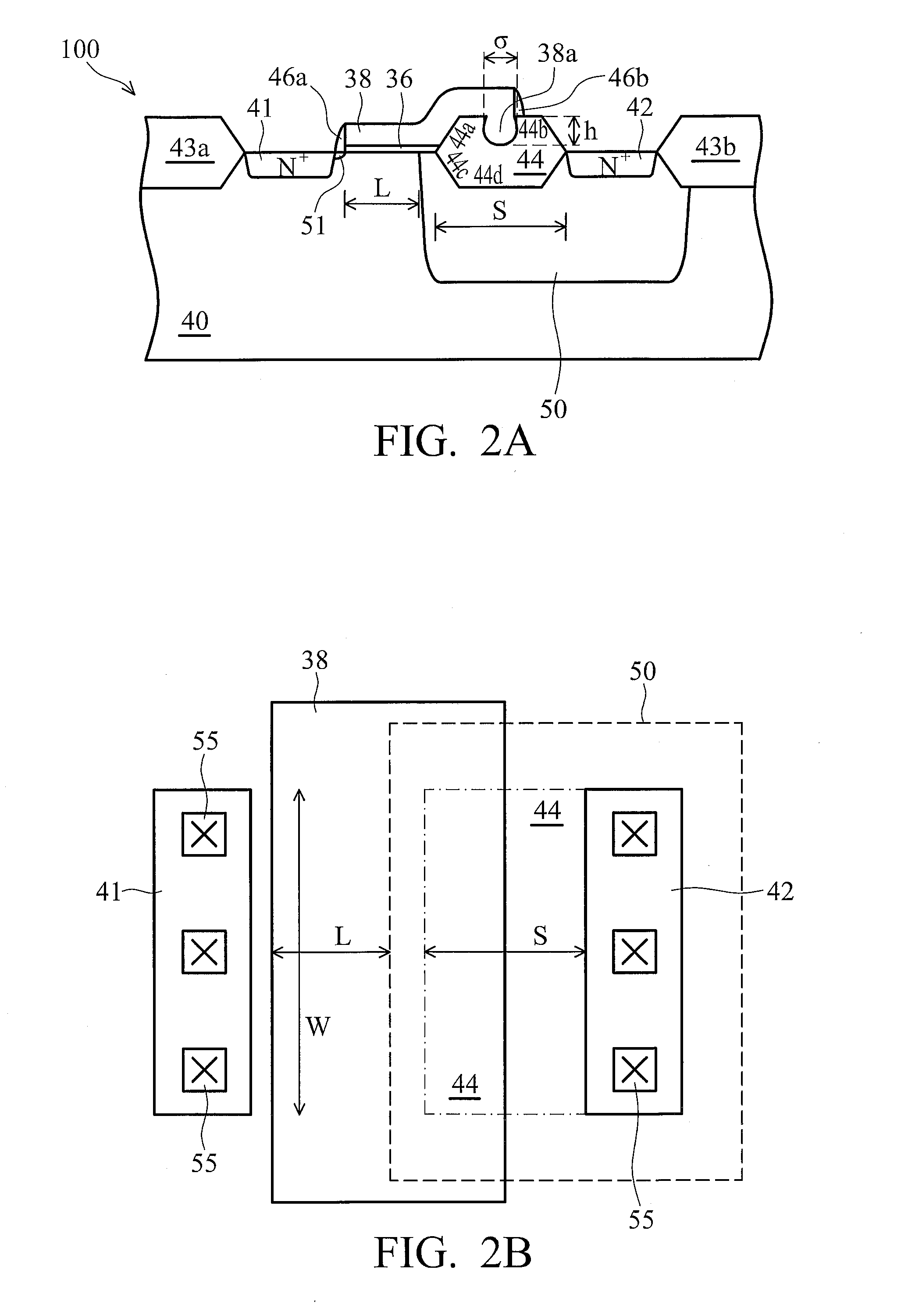
[0017]The present invention will be described with respect to preferred embodiments in a specific context, namely a high voltage LDMOS transistor having a novel structure to suppress hot carrier effect, and the method of forming the same. Embodiments of the present invention may also be applied, however, to other transistor structures and methods of fabrication thereof. While only one transistor is shown in each figure, there may be many transistors formed simultaneously on a single semiconductor workpiece.

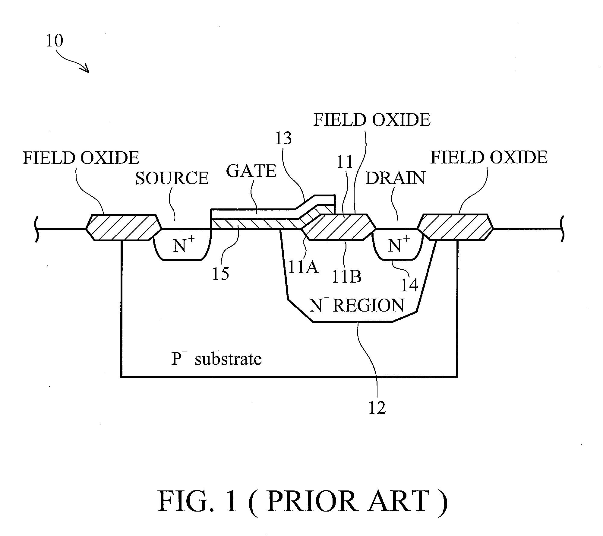
[0018]FIG. 1 shows a cross-sectional view of a prior art high voltage ...


PUM


Abstract

An LDMOS transistor structure and methods of making the same are provided. The structure includes a gate electrode extended on an upper boundary of an extension dielectric region that separates the gate electrode from the drain region of the LDMOS transistor. Moreover, at an area close to an edge of the extended gate electrode portion, the gate electrode further projects downwards into a convex-shaped recess or groove in the upper boundary of the extension dielectric region, forming a tongue. LDMOS transistors with this structure may provide improved suppression of hot carrier effects.

Description

TECHNICAL FIELD[0001]The present invention relates generally to structures of high voltage LDMOS transistors and methods of making the same, and more particularly to high voltage LDMOS transistors with a gate electrode projection, and methods of fabricating the same.BACKGROUND[0002]High voltage MOS transistors are semiconductor devices that can operate with high terminal voltages. High-voltage integrated circuits (ICs) that include high voltage MOS transistors are widely used in applications for the automobile industry, display drivers, portable telecommunication devices, medical equipment, and other areas. As an example, high voltage (e.g., greater than 20 volts) MOS transistors are integrated into a gate driver IC to deliver display signals to a liquid crystal display (LCD) panel. However, with the continuous process shrinking in advanced technology, breakdown voltages of these high voltage MOS transistors are also reduced.[0003]Electric breakdown in MOS transistors is a well reco...

Claims


Application Information

Patent Timeline
Patent Type & Authority Applications(United States)
IPC IPC(8): H01L29/78
CPCH01L27/092H01L29/402H01L29/4236H01L29/7835H01L29/42376H01L29/66659H01L29/7834H01L29/42368
Inventor TIEN, WILLIAM WEI-YUANTSENG, CHAO-WEICHEN, FU-HSIN
Owner TAIWAN SEMICON MFG CO LTD
Why Eureka
Try Eureka