Electroluminescent Displays
- Summary
- Abstract
- Description
- Claims
- Application Information
AI Technical Summary
Benefits of technology
Problems solved by technology
Method used
Image

Examples
Embodiment Construction
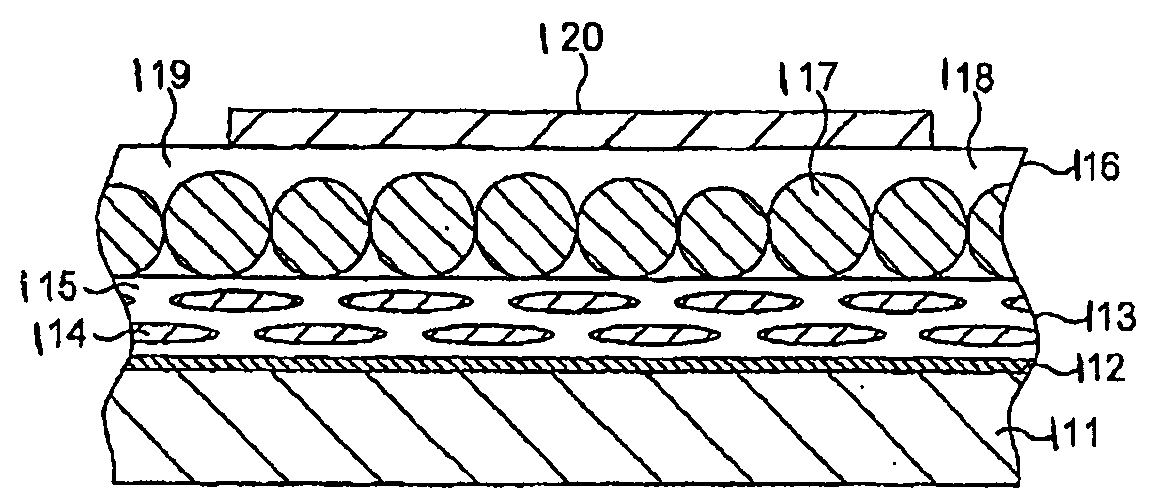
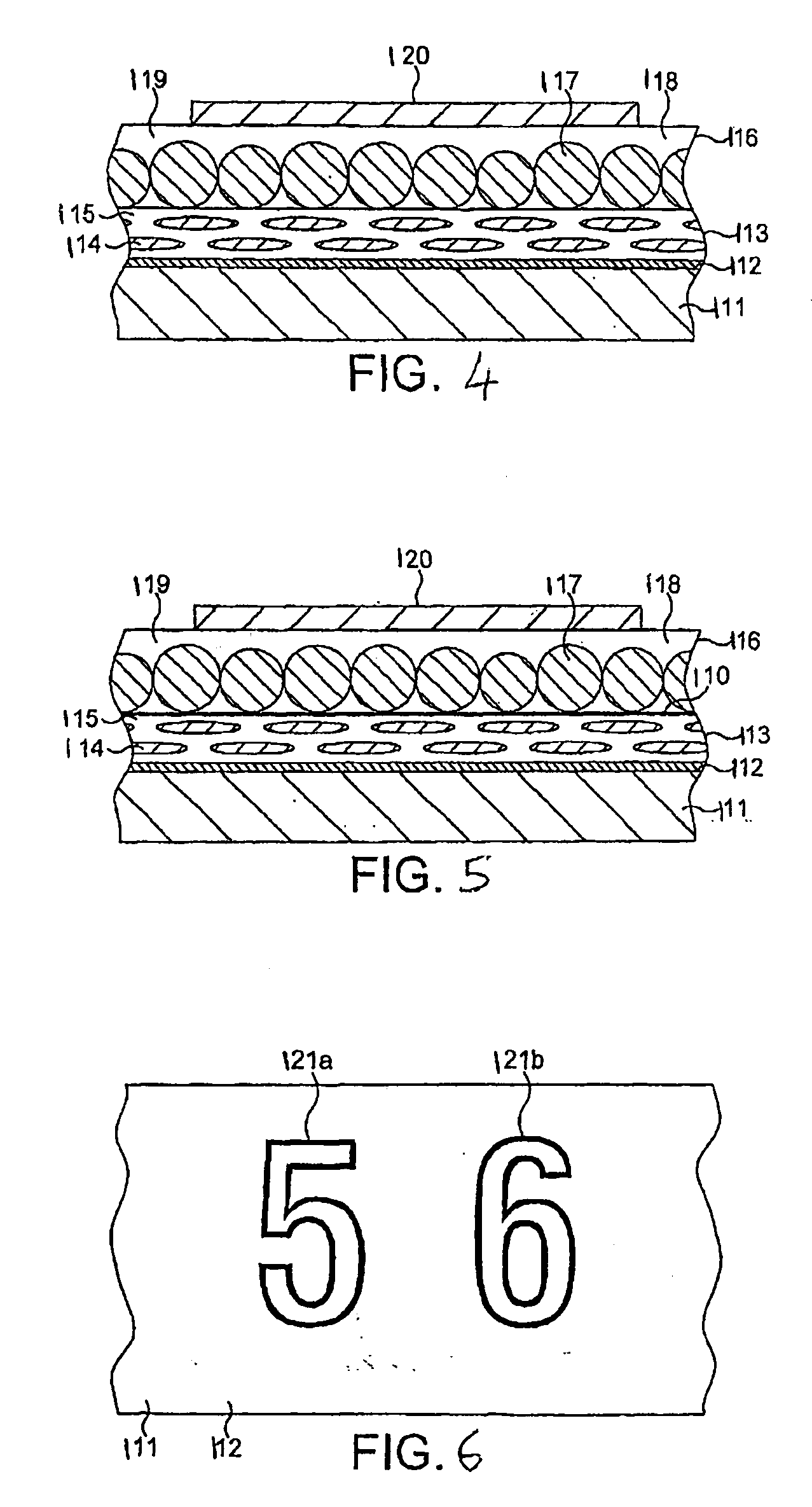
[0112]The structure of the first embodiment of the display of the invention depicted in FIG. 1 of the accompanying drawings can be seen to be, from front to back:[0113]a relatively thick protective electrically-insulating transparent front layer (11; the substrate;[0114]over the rear face of the substrate 11, a relatively thin transparent electrically-conductive film (12) forming the front electrode of the display;[0115]covering the rear face of the front electrode 12, a relatively thin layer (13) of LC material (14) physically-stabilised by being dispersed within a supporting matrix (15);[0116]formed directly on, and covering the rear face of, the liquid crystal layer 13, a relatively thin layer (16) of electroluminescent / phosphor material (17) dispersed within a supporting matrix (18);[0117]over the rear face of the phosphor layer 16, a relatively thin optically-reflective electrically-insulating layer (19) of a relatively high dielectric constant material (in the Figure this laye...
PUM
| Property | Measurement | Unit |
|---|---|---|
| Temperature | aaaaa | aaaaa |
| Fraction | aaaaa | aaaaa |
| Time | aaaaa | aaaaa |
Abstract
Description
Claims
Application Information
 - R&D Engineer
- R&D Manager
- IP Professional
- Industry Leading Data Capabilities
- Powerful AI technology
- Patent DNA Extraction
Browse by: Latest US Patents, China's latest patents, Technical Efficacy Thesaurus, Application Domain, Technology Topic.
© 2024 PatSnap. All rights reserved.Legal|Privacy policy|Modern Slavery Act Transparency Statement|Sitemap