Semiconductor device and method for fabricating the same

a technology of semiconductor devices and semiconductors, applied in semiconductor devices, semiconductor/solid-state device details, electrical apparatus, etc., can solve the problems of electromigration failure and deterioration of the electromigration resistance of the interconnect, and achieve the effect of increasing the effective mechanical strength of the interconnection structure, increasing the electromigration resistance, and reducing the capacitan

Active Publication Date: 2009-11-12
PANNOVA SEMIC
View PDF4 Cites 12 Cited by
  • Summary
  • Abstract
  • Description
  • Claims
  • Application Information

AI Technical Summary

Benefits of technology

[0018]This structure increases the effective mechanical strength of the interconnection structures located around the vias, resulting in an increase in electromigration resistance.
[0019]Furthermore, the local increase in the thickness of the liner insulating film reduces the capacitance between the interconnects.
[0020]In preferred embodiments described later, the liner insulating film is a multilayer film including a first liner insulating film and a second liner insulating film. In those embodiments, the first liner insulating film is not formed outside the via-adjacent regions, and has a Young's modulus of 40 GPa or higher. The second liner insulating film has a dielectric constant of 4.5 or lower. This enables proper adjustment of the balance between increase in electromigration resistance and reduction in the capacitance between the interconnects.
[0021]In another preferred embodiment described later, an air gap is formed between at least one of adjacent pairs of the first interconnects. This reduces the capacitance between the interconnects. The air gap is formed in a gap formed between the one of the adjacent pairs of the first interconnects, and the second liner insulating film is formed on the bottom and side walls of the gap. This enables the air gap to be formed without increasing the number of fabrication process steps, allowing the semiconductor device to be fabricated in a simplified manner.
[0022]In the inventive semiconductor device, preferably, each of the via-adjacent regions is a region on the upper surface of the first interlayer insulating film, has a length and a width each equal to, or within, two to ten times greater than the diameter of a corresponding one of the vias, and has a center matching the center of the corresponding via. This reduces the capacitance between the interconnects, while effectively increasing electromigration resistance.
[0024]In the inventive semiconductor device, of the part of the liner insulating film formed outside the via-adjacent regions, a part formed on a distance between an adjacent pair of the first interconnects which is 2d or more preferably has a greater thickness than a part formed on a distance between an adjacent pair of the first interconnects which is less than 2d, where d is the value of a smallest distance between adjacent pairs of the first interconnects. As in this case, when the distance between interconnects is sufficiently large, the capacitance between those interconnects does not increase. Thus, it is possible to further increase electromigration resistance by employing the above-described structure.

Problems solved by technology

However, the conventional technique has a problem in that the electromigration resistance of interconnects deteriorates.
In this way, electromigration causes a failure.

Method used


Image

  • Semiconductor device and method for fabricating the same
  • Semiconductor device and method for fabricating the same
  • Semiconductor device and method for fabricating the same

Examples


first embodiment

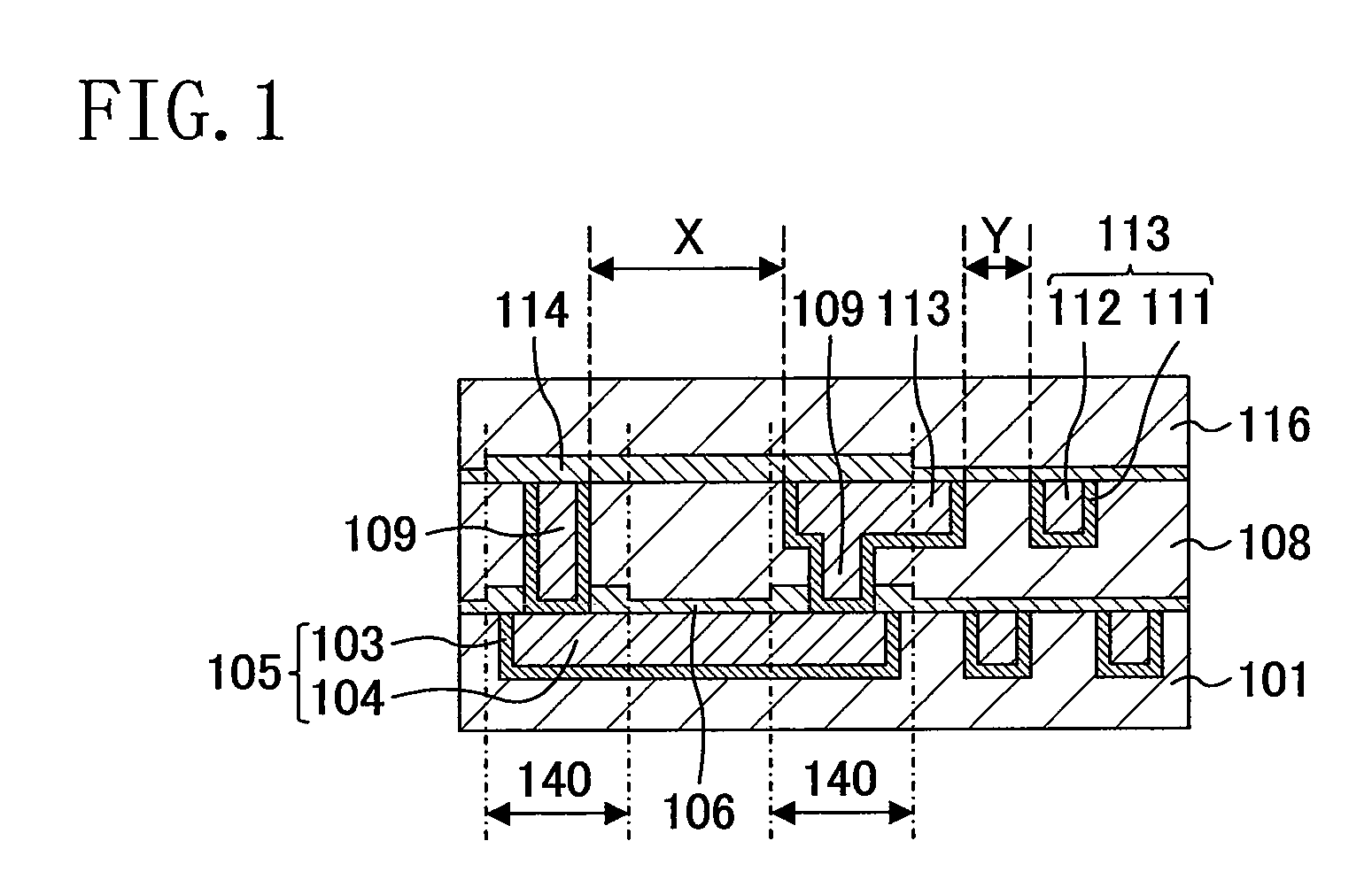
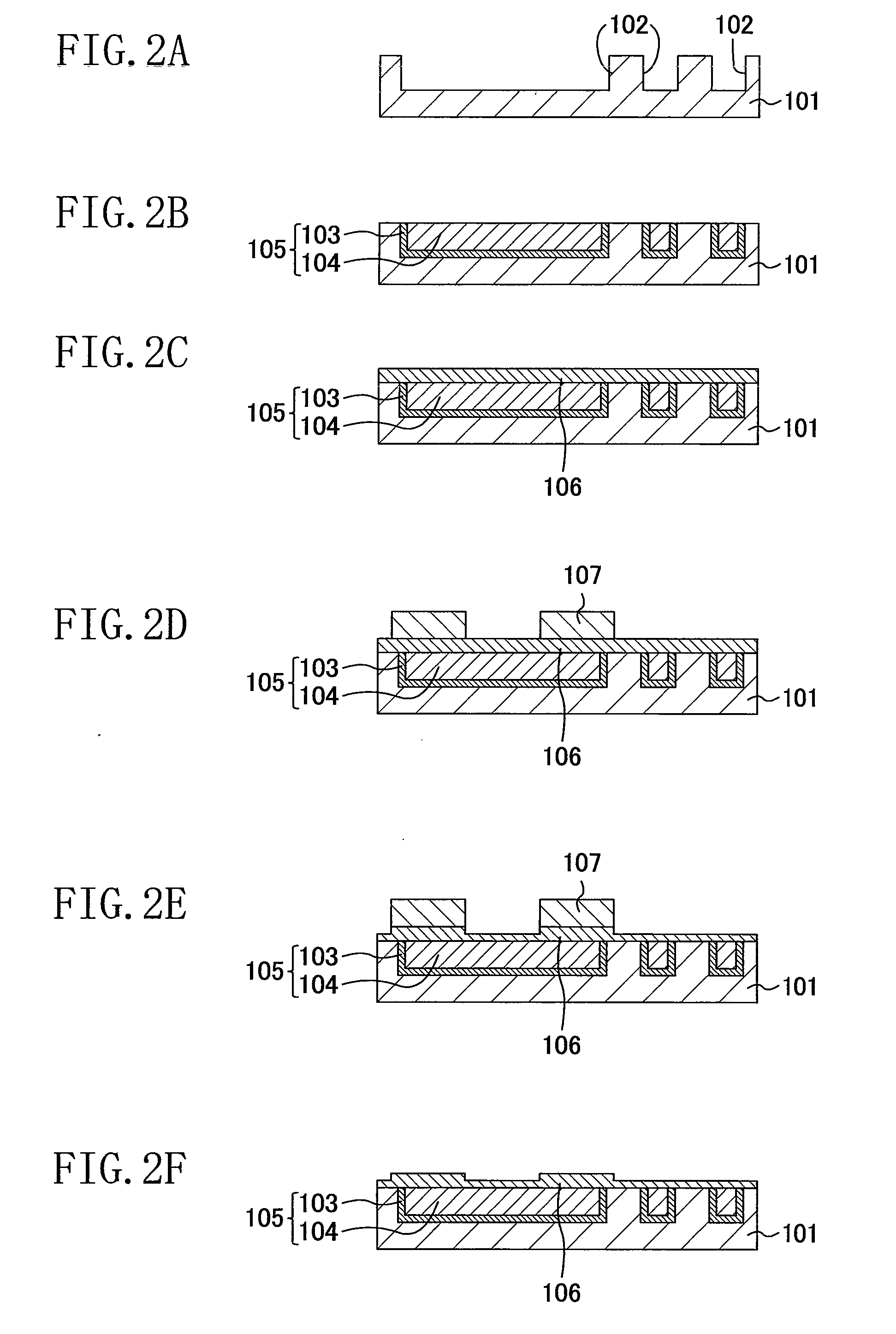
[0055]A semiconductor device according to a first embodiment of the present invention will be described with reference to FIG. 1. It is to be understood that materials and numerical values cited below are only preferable examples, and the present invention is not limited to these materials and numerical values.

[0056]As shown in FIG. 1, lower-level interconnects 105 (first interconnects) are formed in an interlayer insulating film 101 (a first interlayer insulating film) formed on a semiconductor substrate (not shown). A liner insulating film 106 is formed on the interlayer insulating film 101 and lower-level interconnects 105. On the liner insulating film 106, an interlayer insulating film 108 (a second interlayer insulating film) is formed. Vias 109, which are electrically connected with the lower-level interconnects 105, are formed in the liner insulating film 106 and interlayer insulating film 108. In the interlayer insulating film 108, upper-level interconnects 113 (second inter...

second embodiment

[0086]A semiconductor device according to a second embodiment of the present invention will be described with reference to FIG. 5. It should be noted that materials and numerical values cited below are only preferable examples, and the present invention is not limited to these materials and numerical values.

[0087]In the semiconductor device according to this embodiment, liner insulating films 141 and 142 are multilayer films. In the following description, differences from the first embodiment will be mainly discussed.

[0088]As shown in FIG. 5, lower-level interconnects 105 are formed in an interlayer insulating film 101 formed on a semiconductor substrate (not shown). A first liner insulating film 117 is formed on the interlayer insulating film 101 and lower-level interconnect 105. A second liner insulating film 119 is formed over the first liner insulating film 117. The first and second liner insulating films 117 and 119 form the liner insulating film 141. On the second liner insula...

third embodiment

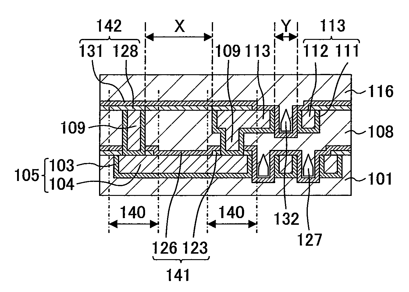
[0121]A semiconductor device according to a third embodiment of the present invention will be described with reference to FIG. 9. It should be noted that materials and numerical values cited below are only preferable examples, and the present invention is not limited to these materials and numerical values.

[0122]In the semiconductor device according to this embodiment, air gaps 127 are formed between adjacent lower-level interconnects 105 and 105, and air gaps 132 are formed between adjacent upper-level interconnects 113 and 113.

[0123]As shown in FIG. 9, lower-level interconnects 105 are formed in an interlayer insulating film 101 formed on a semiconductor substrate (not shown). A first liner insulating film 123 is formed on the interlayer insulating film 101 and lower-level interconnects 105. A second liner insulating film 126 is formed over the first liner insulating film 123. The first and second liner insulating films 123 and 126 form a liner insulating film 141. An interlayer i...


PUM


Abstract

An interlayer insulating film is formed on the upper surface of a semiconductor substrate, and lower-level interconnects are formed in the interlayer insulating film. A liner insulating film is formed on the upper surfaces of the interlayer insulating film and lower-level interconnects. An interlayer insulating film is formed on the upper surface of the liner insulating film. Upper-level interconnects are formed in the interlayer insulating film. The lower-level interconnects and the upper-level interconnects are connected with each other through vias. Parts of the liner insulating film formed in via-adjacent regions have a greater thickness than a part thereof formed outside the via-adjacent regions.

Description

CROSS REFERENCE TO RELATED APPLICATION[0001]This application claims priority from Japanese Patent Application No. 2008-125135 filed on May 12, 2008, which is hereby incorporated by reference in its entirety for all purposes.BACKGROUND OF THE INVENTION[0002]The present invention relates to a semiconductor device and a method for fabricating the semiconductor device.[0003]In recent years, with the increasing miniaturization of semiconductor integrated circuit devices, the distance between interconnects that connect semiconductor integrated circuit devices, and the distance between interconnects formed in semiconductor integrated circuit devices have been reduced. Due to this, a problem has emerged in that the capacitance between interconnects increases causing a reduction in signal transmission speed. In light of this, as described in pp. 213-215 in “45 nm Node Multi Level Interconnects with Porous SiOCH Dielectric k=2.5” by V. Arnal et, al. (IITC2006), methods for reducing the capaci...

Claims


Application Information

Patent Timeline
Patent Type & Authority Applications(United States)
IPC IPC(8): H01L23/522H01L21/768
CPCH01L21/7682H01L21/76829H01L21/76832H01L21/76834H01L23/5222H01L2924/0002H01L23/53238H01L23/53295H01L2924/00
Inventor HARADA, TAKESHISHIBATA, JUNICHIUEKI, AKIRA
Owner PANNOVA SEMIC
Why Eureka
Try Eureka